Why HDI PCBs Are No Longer Optional
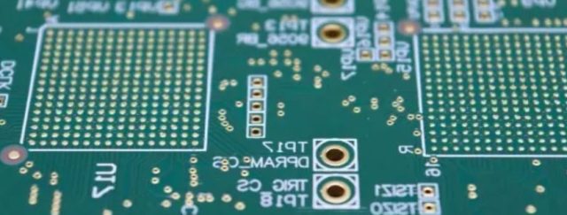
As electronic devices become smaller, faster, and more complex, traditional multilayer PCB designs struggle to keep up. HDI (High-Density Interconnect) PCBs address this challenge by enabling higher routing density, shorter signal paths, and better electrical performance.
At the core of HDI technology is the use of:
- Microvias (laser-drilled vias)
- Blind and buried vias
- Fine line and spacing geometries
These features allow designers to break routing limitations imposed by conventional through-hole PCB designs. In modern applications—especially mobile devices, high-speed computing, and semiconductor testing—HDI is often not a luxury, but a necessity.
Interconnect Strategy: The Real Value of HDI
HDI is not just about density—it is about how signals move through the board.
- Microvia-Based Routing:
Microvias enable direct layer-to-layer connections, significantly reducing signal path length. - Sequential Lamination:
Multiple lamination cycles allow complex via structures such as stacked and staggered microvias. - Via-in-Pad Technology:
Allows routing directly from component pads, especially for fine-pitch BGAs. - Layer Utilization Efficiency:
HDI reduces the need for excessive layers by improving routing efficiency per layer.
This results in a PCB architecture that is more compact, more efficient, and electrically optimized.
Signal & Density Benefits
HDI PCBs provide measurable improvements in both electrical performance and physical design:
- Improved Signal Integrity (SI):
Shorter interconnects reduce reflections, insertion loss, and timing skew. - Better Power Integrity (PI):
Optimized routing allows more effective power distribution networks with lower impedance. - Reduced Crosstalk:
Fine routing and improved layer separation minimize interference between signals. - Higher Component Density:
Supports advanced packages such as fine-pitch BGA, CSP, and flip-chip devices. - Smaller Form Factor:
Enables compact product designs without sacrificing functionality.
For high-speed designs (PCIe, DDR, SerDes), HDI can significantly improve overall system performance.
Manufacturing Trade-Offs
While HDI offers clear advantages, it introduces complexity that must be carefully managed:
- Cost Increase:
Laser drilling, sequential lamination, and fine-line processing add manufacturing cost. - Yield Sensitivity:
Stacked microvias and fine features require tight process control to maintain yield. - Thermal Reliability:
Improperly designed microvias can fail under thermal cycling if not optimized. - Design-Manufacturing Alignment:
Close collaboration with the PCB manufacturer is essential during stack-up and via planning. - Inspection & Testing:
Advanced QA methods (X-ray, microsectioning, impedance testing) are required to ensure reliability.
At KKPCB, we mitigate these challenges through process optimization, strict QA, and DFM support, ensuring HDI designs are both manufacturable and reliable.
When Should You Use HDI?
HDI PCBs are most valuable when conventional designs reach their limits. You should consider HDI when:
- Routing becomes congested in standard multilayer boards
- Using fine-pitch BGA or high pin count components
- Designing high-speed digital systems
- Building compact consumer or portable devices
- Developing ATE, probe cards, or advanced test hardware
In many cases, HDI is not just about making boards smaller—it is about making complex designs feasible.
Final Thoughts
HDI PCBs represent a shift from traditional PCB design to precision interconnect engineering. By leveraging microvias, fine routing, and optimized stack-ups, engineers can achieve higher performance, greater density, and improved reliability.
At KKPCB, we support HDI PCB development with advanced fabrication capabilities, design guidance, and rigorous quality control, helping customers bring high-performance electronic products to market efficiently and reliably.
