Why Buried Vias Matter
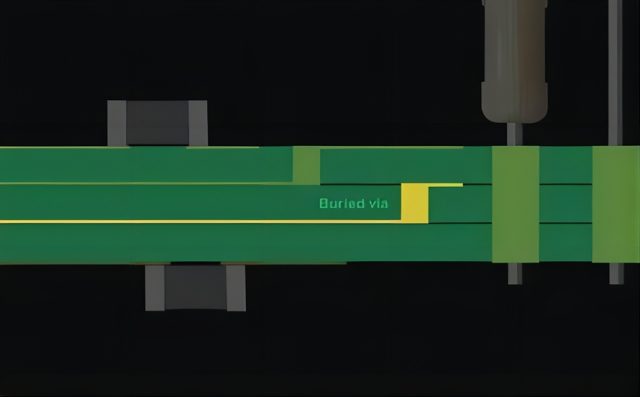
As electronic systems become more compact and performance-driven, traditional via structures are no longer sufficient for complex routing requirements. A Buried Via PCB enables connections only between internal layers, eliminating unnecessary vertical paths through the entire board.
This design approach is not just about saving space—it is about engineering control over signal paths, layer utilization, and electrical behavior. In high-speed and high-density designs, every via transition introduces parasitic effects. Buried vias help minimize these effects by keeping interconnections localized and efficient.
Architecture Strategy in Multilayer Design
Buried vias play a critical role in modern multilayer PCB architecture. Instead of treating vias as simple vertical connections, engineers use them as strategic routing tools.
In advanced stack-ups:
- Inner signal layers are interconnected without disturbing outer-layer routing
- Power and ground planes remain continuous, improving return paths
- RF and high-speed signals can be isolated from noisy digital layers
This allows designers to build cleaner layer hierarchies, where each layer has a defined function—RF, high-speed digital, power distribution, or shielding.
Buried vias are often combined with blind vias and microvias in HDI designs, creating a layered interconnect system that maximizes routing efficiency while maintaining electrical performance.
Performance Impact on High-Speed Designs
From a signal integrity perspective, buried vias provide several measurable benefits:
- Reduced Stub Effect:
Unlike through-hole vias, buried vias eliminate unused via stubs, which can cause signal reflections in high-speed circuits. - Lower Parasitic Effects:
Shorter vertical paths reduce parasitic capacitance and inductance, improving signal quality. - Improved Return Path Continuity:
Maintaining uninterrupted reference planes enhances signal stability and reduces EMI. - Better High-Frequency Behavior:
In RF and microwave designs, minimizing discontinuities is critical—buried vias help preserve impedance consistency.
For engineers working with multi-gigabit signals or GHz frequencies, these improvements directly translate into cleaner eye diagrams and lower insertion loss.
Manufacturing Reality: What Engineers Must Know
While buried vias offer clear design advantages, they also introduce manufacturing complexity that must be considered early in the design phase.
- Sequential Lamination:
Buried vias require inner layers to be fabricated and laminated before adding outer layers, increasing process steps. - Registration Accuracy:
Layer-to-layer alignment must be extremely precise, especially in high layer count boards. - Inspection Challenges:
Since buried vias are enclosed, verification relies on X-ray and cross-section analysis rather than visual inspection. - Cost vs Benefit Trade-Off:
The added fabrication complexity increases cost, so buried vias should be used where they deliver clear performance or density advantages.
Working closely with the PCB manufacturer—especially during stack-up planning—is essential to ensure that the design is both manufacturable and reliable.
When Should You Use Buried Vias?
Buried vias are not necessary for every PCB design. Their value becomes clear in specific scenarios:
- High Layer Count PCBs (10+ layers)
- HDI designs with limited routing space
- High-speed digital systems (PCIe, DDR, SerDes)
- RF and microwave circuits requiring impedance stability
- Compact products where board size must be minimized
If your design is constrained by routing congestion or signal integrity issues, buried vias can provide a targeted solution without overcomplicating the entire board.
Final Thoughts
Buried via PCBs are not just a manufacturing feature—they are a design strategy for optimizing multilayer performance. When applied correctly, they enable engineers to:
- Improve routing efficiency
- Enhance signal integrity
- Reduce interference
- Maintain compact form factors
At KKPCB, we support complex multilayer and HDI designs with advanced via technologies, precise lamination control, and rigorous quality assurance, helping engineers bring high-performance products to market with confidence.
