As modern electronics push higher frequencies and data rates, high-frequency (HF) multilayer PCBs have become essential in enabling reliable and precise signal transmission. These PCBs are used in applications where low dielectric loss, controlled impedance, and minimal signal reflection are critical.
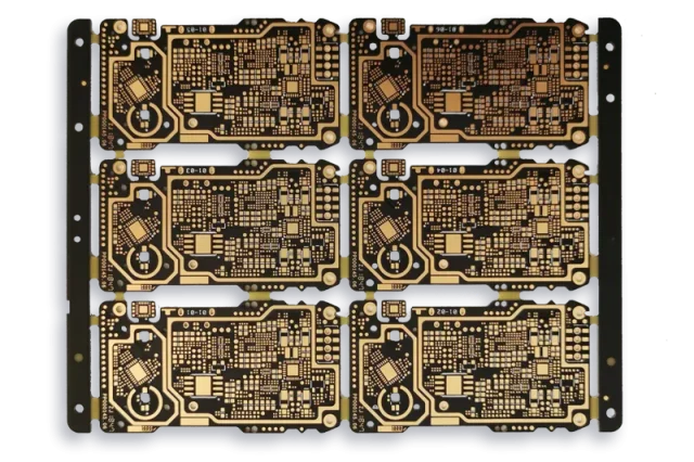
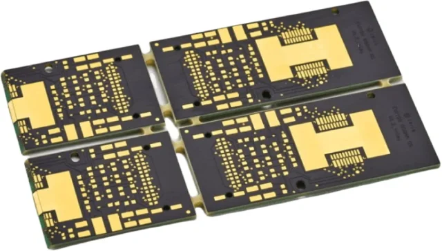
Multilayer HF PCBs combine multiple layers of conductive and dielectric materials to achieve high-density interconnections, while maintaining excellent signal integrity across RF and microwave frequencies.
What is a Multilayer HF PCB?
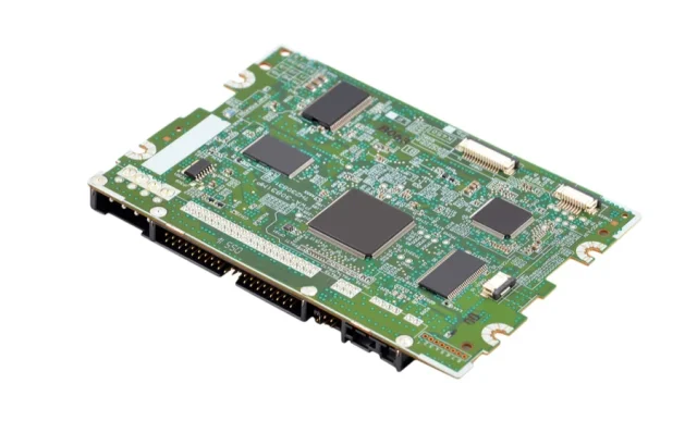
A Multilayer HF PCB is a printed circuit board designed for high-frequency and high-speed electronic applications. It integrates multiple layers of copper traces separated by low-loss dielectric substrates to support complex circuit routing while maintaining RF performance.
Key characteristics include:
-
Low dielectric loss for high-frequency signals
-
Controlled impedance for signal integrity
-
High-density multilayer structure for complex circuit routing
-
Thermal stability for consistent performance in demanding environments
These features make multilayer HF PCBs ideal for RF, microwave, and high-speed digital applications.
Advantages of Multilayer HF PCB
1. High-Frequency Signal Integrity
Multilayer HF PCBs provide precise impedance control and reduced signal loss, critical for RF circuits, antennas, and high-speed digital modules.
2. Compact High-Density Design
Multiple layers allow designers to route complex circuits in a compact form factor, reducing board size while supporting advanced electronic functionality.
3. Improved Thermal Management
Stack-up designs can include dedicated power and ground planes, which help dissipate heat generated by high-speed components, ensuring long-term reliability.
4. Enhanced Electromagnetic Compatibility (EMC)
Multilayer configurations allow for better shielding and ground plane design, reducing crosstalk and electromagnetic interference in high-frequency circuits.
Key Applications of Multilayer HF PCB
Multilayer HF PCBs are widely used in industries that demand high-speed and high-frequency performance:
-
Wireless communication devices (5G, Wi-Fi, IoT modules)
-
Radar and satellite communication systems
-
Automotive radar and ADAS modules
-
RF amplifiers and microwave circuits
-
High-speed computing and server systems
These applications rely on the PCB’s ability to maintain low loss and precise impedance across multiple layers.
Design Considerations for Multilayer HF PCB
-
Material Selection
-
Low-loss laminates such as Rogers, PTFE, or high-frequency FR-4 variants.
-
Stable dielectric constant (Dk) for controlled impedance.
-
-
Stack-Up Design
-
Optimal layer arrangement for signal routing, power distribution, and ground planes.
-
Proper separation of high-speed signals from power traces to minimize interference.
-
-
Impedance Control
-
Controlled trace width, spacing, and via design to maintain signal integrity.
-
-
Thermal and Mechanical Reliability
-
Thermal vias, copper planes, and proper material selection to handle high-frequency operation and heat dissipation.
-
Manufacturing Considerations
Producing multilayer HF PCBs requires advanced fabrication processes:
-
Precision etching and lamination to maintain tight tolerances
-
Accurate layer alignment for multilayer stack-ups
-
High-quality via drilling and plating for reliable interconnects
-
Rigorous testing for impedance, signal loss, and high-frequency performance
Reliable manufacturing ensures the PCB meets the high-speed and high-frequency requirements of advanced electronic systems.
Conclusion
Multilayer HF PCBs are critical for high-frequency, high-speed electronic applications. With precise impedance control, low signal loss, and advanced multilayer designs, these PCBs support modern RF modules, radar systems, 5G devices, and complex digital circuits.
Choosing the right materials, stack-up, and fabrication process is key to delivering high-performance, reliable multilayer HF PCBs for next-generation electronic systems.
