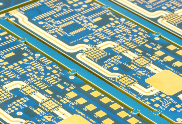
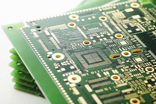
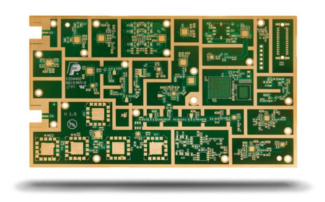
What Is a Low Loss PCB?

A Low Loss PCB is a printed circuit board designed using low dielectric loss materials to minimize signal attenuation during high-speed or high-frequency transmission.
As data rates increase and RF frequencies enter the multi-GHz range, signal integrity becomes highly sensitive to material loss. Low loss PCB materials help preserve signal strength and reduce distortion across long routing distances.
Understanding Signal Loss in PCB Design
Signal loss in PCBs primarily comes from two sources:
-
Conductor Loss – Resistance of copper traces
-
Dielectric Loss – Energy dissipated within the substrate material
At higher frequencies, dielectric loss becomes increasingly dominant. The key material parameter controlling this is the dissipation factor (Df).
Lower Df means lower signal attenuation.
Key Characteristics of Low Loss PCB Materials
Low loss PCB materials typically feature:
-
Low dissipation factor (Df ≤ 0.005 or lower)
-
Stable dielectric constant (Dk) across frequency
-
Low moisture absorption
-
High dimensional stability
These properties ensure consistent impedance and reduced insertion loss.
Why Low Loss PCB Is Important for High-Speed Design
In high-speed digital systems such as:
-
10G / 25G / 56G Ethernet
-
PCIe Gen4 / Gen5
-
DDR4 / DDR5 memory
-
AI accelerator boards
Signal edges are extremely fast. Even small material losses can significantly impact eye diagram performance and channel budget.
Low loss PCB materials extend signal reach and improve overall system reliability.
Low Loss PCB in RF and Microwave Applications
For RF circuits operating in the GHz range:
-
Insertion loss directly affects amplifier efficiency
-
Phase stability impacts antenna performance
-
Material consistency ensures predictable filter behavior
Manufacturers such as Rogers Corporation and Taconic provide specialized low-loss laminates widely used in microwave PCB fabrication.
Design Considerations for Low Loss PCB
To maximize performance, engineers should consider:
1. Controlled Impedance Stack-Up
Precise layer configuration is essential for stable transmission lines.
2. Surface Roughness Control
Smoother copper reduces conductor loss at high frequency.
3. Via Optimization
Back-drilling or microvias help reduce stub-induced reflections.
4. Hybrid Material Structures
Combining low-loss laminate for signal layers and FR4 for non-critical layers can optimize cost.
Low Loss PCB vs Standard FR4 PCB
| Feature | Standard FR4 | Low Loss PCB |
|---|---|---|
| Dissipation Factor | Higher | Lower |
| High-Frequency Stability | Moderate | Excellent |
| Signal Attenuation | Higher | Reduced |
| Cost | Lower | Higher |
| Application Range | General Electronics | High-Speed / RF |
Low loss PCB is essential when signal performance outweighs material cost.
Typical Applications
Low Loss PCBs are widely used in:
-
5G infrastructure equipment
-
Data center networking hardware
-
High-speed computing systems
-
Radar and satellite systems
-
Aerospace communication platforms
-
Automotive high-speed ADAS modules
As bandwidth demands grow, low loss PCB solutions become increasingly important.
Conclusion
Low Loss PCB technology enables stable, long-distance, and high-frequency signal transmission in modern electronic systems. By reducing dielectric loss and maintaining impedance stability, it ensures reliable performance in both high-speed digital and RF applications.
For advanced communication and computing systems, selecting low loss PCB materials is a critical engineering decision.
