What Is a Buried Via PCB?
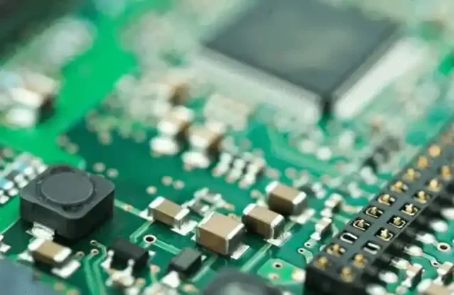
A Buried Via PCB is a multilayer printed circuit board that uses vias connecting only internal layers, without extending to the outer surface layers. Unlike through-hole vias that pass through the entire board thickness, buried vias are fully embedded within the PCB stack-up.
This structure improves routing density, reduces surface congestion, and enhances signal performance in complex electronic designs.
Buried via technology is commonly used in high-layer-count and HDI PCBs where space optimization and signal integrity are critical.
Advantages of Buried Via PCB
1. Increased Routing Density
By connecting internal layers directly, buried vias free up valuable surface space for:
-
Fine pitch components
-
High pin count BGA packages
-
Dense signal routing
This enables more compact and efficient board layouts.
2. Improved Signal Integrity
Because buried vias do not extend through the entire board, they:
-
Reduce via stubs
-
Minimize signal reflection
-
Lower parasitic capacitance and inductance
This is particularly important for high-speed and high-frequency applications.
3. Better Layer Utilization
Buried vias allow more efficient use of internal layers, improving:
-
Power plane distribution
-
Ground reference continuity
-
Signal layer optimization
This enhances overall electrical performance.
4. Reduced Board Thickness (in Some Designs)
By optimizing layer interconnections, designers may reduce overall board thickness while maintaining routing capability.
Buried Via vs Through-Hole Via
| Feature | Through-Hole Via | Buried Via |
|---|---|---|
| Connection | All layers | Internal layers only |
| Surface Occupancy | Uses surface space | Hidden inside |
| Via Stub | Present | Minimized |
| Routing Density | Moderate | High |
| Manufacturing Complexity | Lower | Higher |
Buried via PCBs require more advanced lamination processes compared to standard multilayer boards.
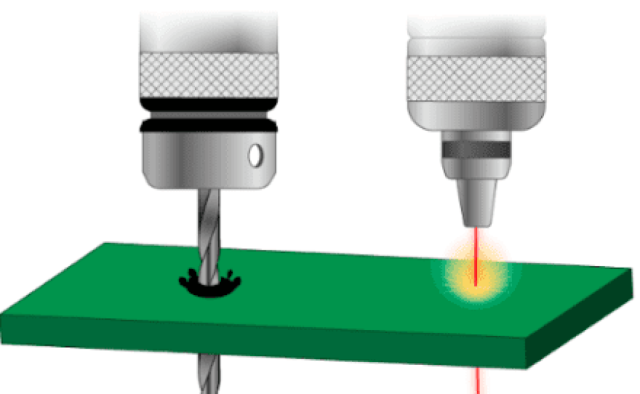
Manufacturing Process
Buried via PCB fabrication typically involves:
-
Sequential lamination
-
Inner layer drilling and plating
-
Multiple pressing cycles
-
Precision layer alignment
-
X-ray inspection for internal structure
Strict process control is essential to ensure accurate registration and reliable interlayer connectivity.
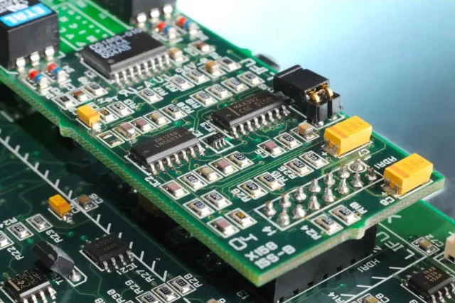
Applications of Buried Via PCB
Buried via PCBs are widely used in:
-
High layer count server boards
-
5G communication systems
-
High-speed networking equipment
-
Semiconductor test boards
-
Automotive electronics
-
Aerospace control systems
-
Industrial automation platforms
In systems requiring complex signal routing and stable impedance control, buried via technology provides significant advantages.
Design Considerations
When designing a buried via PCB, engineers must consider:
-
Stack-up structure planning
-
Via aspect ratio
-
Thermal reliability
-
Impedance control
-
Manufacturing tolerances
Close collaboration between design engineers and PCB manufacturers helps optimize performance and yield.
Conclusion
Buried Via PCB technology enables higher routing density, improved signal integrity, and more efficient multilayer design. By embedding vias within internal layers, designers gain greater flexibility for high-speed and high-density electronic systems.
For advanced communication, computing, automotive, and industrial applications, buried via PCBs provide a reliable and high-performance interconnection solution.
