What Is an RF Trace PCB?
An RF Trace PCB is a printed circuit board designed with optimized RF trace routing to carry radio frequency (RF) signals with minimal loss, stable impedance, and strong EMI control. RF traces are transmission lines that must maintain consistent electrical performance at high frequencies, typically from hundreds of MHz to several GHz.
Unlike standard digital routing, RF trace PCB design focuses on controlling impedance, insertion loss, return loss, radiation, coupling, and noise, ensuring reliable performance in applications such as 5G communication, WiFi, Bluetooth, GPS, IoT devices, RF modules, and radar systems.
A well-designed RF Trace PCB improves signal quality, reduces interference, and ensures stable RF performance in compact and high-density layouts.
Why RF Trace PCB Design Matters
At RF frequencies, even small layout changes can significantly affect circuit performance. Poor RF trace design may cause:
-
Impedance mismatch and signal reflection
-
Higher insertion loss and reduced transmission efficiency
-
Increased EMI radiation and interference
-
Frequency shift and unstable tuning
-
Poor antenna matching and reduced range
-
Noise coupling into sensitive RF sections
That is why RF Trace PCB routing must be treated as a critical part of the RF system design.
Key Features of an RF Trace PCB
1. Controlled Impedance RF Trace Routing
A high-quality RF Trace PCB requires precise controlled impedance to maintain stable RF transmission. Typical RF trace impedance targets include:
-
50Ω single-ended RF traces
-
75Ω RF traces (common in video/RF systems)
-
100Ω differential RF traces (high-speed RF links)
Controlled impedance helps reduce reflection and ensures consistent RF signal behavior across the PCB.
2. Low Loss PCB Materials for RF Performance
Material selection is critical for RF Trace PCB design. High-frequency circuits often require low loss PCB materials with stable dielectric properties to reduce attenuation.
Common RF PCB materials include:
-
Rogers PCB laminates (RO4003C, RO4350B, RO3003)
-
PTFE / Duroid PCB materials
-
Low-loss high-speed laminates (Megtron series)
Low loss materials help improve RF efficiency and maintain stable performance at high frequencies.
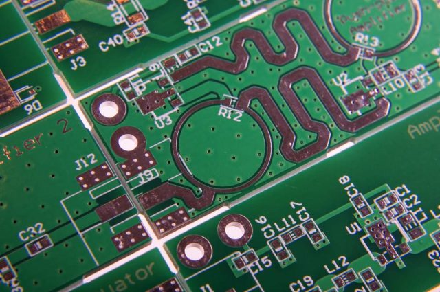
3. RF Trace Geometry and Stack-Up Design
RF traces are commonly designed as:
-
Microstrip RF traces (outer layer with ground reference plane)
-
Stripline RF traces (inner layer between ground planes)
-
Coplanar waveguide (CPW) with ground for improved shielding
A professional RF Trace PCB stack-up ensures stable impedance control and reduces EMI radiation.
4. Grounding and RF Shielding Structures
RF Trace PCB designs rely heavily on strong grounding. Key grounding strategies include:
-
Solid ground planes under RF traces
-
Via stitching around RF lines for shielding
-
Ground fences to reduce radiation
-
Short return paths to minimize loop area
Proper grounding improves RF stability and reduces noise coupling.
5. Minimizing RF Discontinuities
RF traces are sensitive to discontinuities such as:
-
Sharp corners and sudden width changes
-
Poor via transitions and stubs
-
Uncontrolled connectors and launch structures
-
Gaps in reference planes
A well-designed RF Trace PCB uses smooth routing, controlled transitions, and optimized launches to minimize performance degradation.
6. RF Trace Spacing and Isolation
RF signals can easily couple into nearby traces. RF Trace PCB routing should include:
-
Adequate spacing between RF lines and digital signals
-
Isolation from switching power circuits
-
Ground shielding between sensitive traces when needed
-
Proper partitioning of RF and baseband sections
This improves EMI control and overall RF performance.
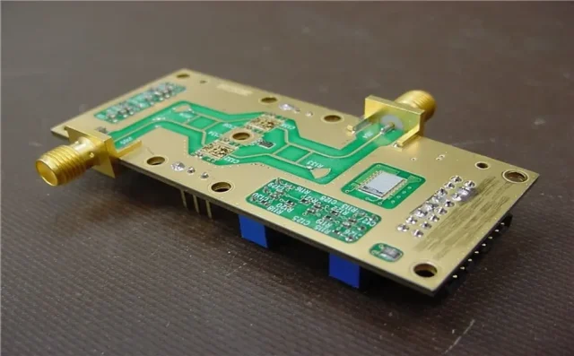
Common Applications of RF Trace PCBs
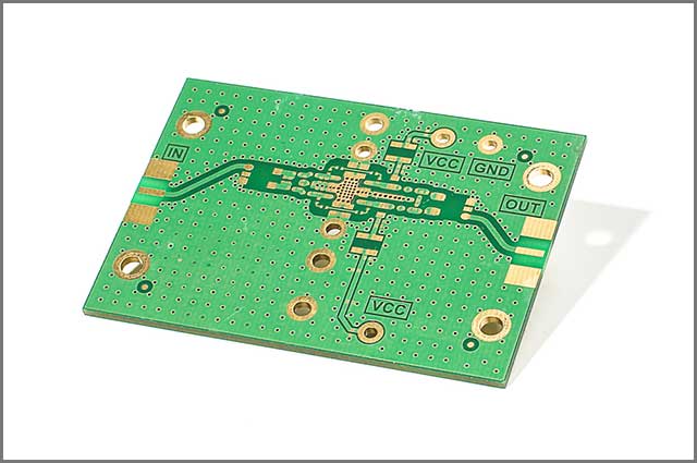
RF Trace PCBs are widely used in:
-
5G RF modules and base stations
-
WiFi and Bluetooth communication devices
-
GPS receivers and navigation systems
-
IoT wireless modules and sensors
-
Automotive radar and ADAS systems
-
Microwave communication equipment
-
RF test boards and measurement devices
-
Satellite communication systems
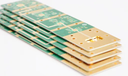
KKPCB RF Trace PCB Manufacturing Capabilities
KKPCB provides professional RF Trace PCB manufacturing with engineering support for high-frequency and RF designs. Our services include:
-
Controlled impedance RF trace fabrication
-
Low loss PCB material options for RF performance
-
Multilayer RF PCB stack-up design support
-
Fine line PCB and HDI PCB for compact RF modules
-
Via stitching and RF shielding structures
-
High reliability PCB processes and inspection
-
Prototype to mass production support
We help customers build RF Trace PCBs with stable impedance, low loss, and consistent RF performance.
Conclusion
An RF Trace PCB is essential for high-frequency and wireless systems, providing controlled impedance, low insertion loss, and stable RF signal transmission. By selecting low loss materials, optimizing stack-up and RF trace geometry, improving grounding and shielding, and minimizing discontinuities, RF Trace PCBs achieve reliable performance for 5G, WiFi, GPS, IoT, and radar applications.
KKPCB delivers high-quality RF Trace PCB solutions with advanced manufacturing capabilities and high reliability production control for demanding RF electronics.
