What Is a Differential Pair PCB?
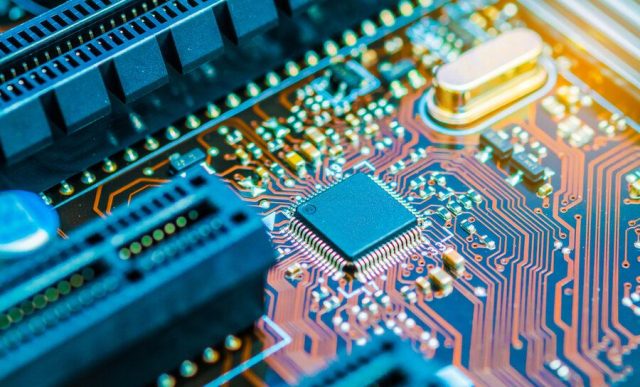
A Differential Pair PCB is a printed circuit board that routes signal pairs with equal and opposite voltages to maintain signal integrity and reduce noise. Differential pairs are essential for high-speed digital interfaces, high-frequency analog signals, and RF communication systems.
By using precisely matched trace lengths, controlled spacing, and proper impedance, Differential Pair PCBs ensure minimal crosstalk, reduced EMI, and reliable high-speed performance.
Why Differential Pair PCBs Are Important
Differential pair routing is critical in high-speed electronics because:
-
It reduces electromagnetic interference (EMI)
-
Maintains signal integrity in high-speed digital and RF circuits
-
Minimizes crosstalk between adjacent signals
-
Improves timing accuracy for high-frequency communication
Applications of Differential Pair PCBs include USB 3.0/3.1, PCIe, SATA, Ethernet, high-speed memory buses, and RF front-end modules.
Key Design Considerations for Differential Pair PCBs
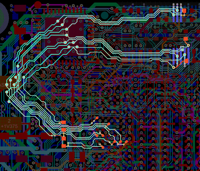
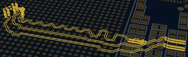
1. Trace Length Matching
Differential pairs must be length-matched to maintain synchronous signal propagation and prevent timing skew.
2. Controlled Impedance
The trace width, spacing, and dielectric material must be designed to achieve consistent differential impedance, typically 90–100 ohms, to reduce reflections and signal degradation.
3. Multilayer Stack-Up Optimization
Placing differential pairs adjacent to ground or power planes ensures stable return paths, reduces noise, and minimizes EMI.
4. Crosstalk Mitigation
Sufficient spacing between differential pairs and other signal traces prevents crosstalk and unwanted signal coupling.
5. Low-Loss Materials
High-frequency signals require low-loss laminates to preserve signal strength and reduce insertion loss in long traces.
6. Termination and Routing Practices
Proper termination resistors and careful routing practices maintain signal fidelity and reduce reflections in high-speed applications.
Applications of Differential Pair PCBs
-
High-speed digital interfaces: USB, PCIe, SATA
-
High-frequency memory and logic buses
-
RF communication and 5G modules
-
High-speed Ethernet and networking equipment
-
IoT devices with high-speed signaling
-
High-performance computing and server boards
KKPCB Differential Pair PCB Capabilities
KKPCB provides professional Differential Pair PCB design and manufacturing services, including:
-
Trace length matching and impedance-controlled routing
-
Multilayer stack-ups with optimized signal, power, and ground planes
-
Low-loss material selection for high-frequency and high-speed signals
-
Crosstalk mitigation and EMI reduction techniques
-
Prototyping and full-scale production with high reliability
Our engineers ensure every Differential Pair PCB meets strict electrical, thermal, and mechanical requirements, delivering high-speed, high-performance, and reliable solutions for industrial, automotive, and RF applications.
Conclusion
A Differential Pair PCB is critical for maintaining signal integrity, minimizing noise, and ensuring reliable high-speed performance in modern electronics. With controlled impedance, precise trace matching, low-loss materials, and optimized multilayer stack-ups, KKPCB provides professional Differential Pair PCB solutions for high-speed digital, RF, 5G, and industrial applications.
