Introduction to High Speed Logic PCB
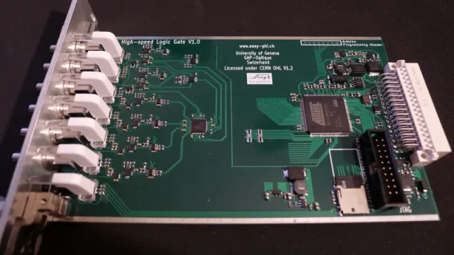
A High Speed Logic PCB is designed to support ultra-fast digital circuits while maintaining signal integrity, low noise, and reliable operation. These PCBs are critical for modern electronics, where data rates and clock frequencies are continually increasing, such as in computing, networking, 5G communications, automotive ECUs, and IoT devices.
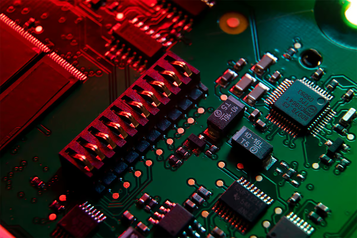
High Speed Logic PCBs are engineered to handle timing-sensitive signals and prevent issues like crosstalk, signal reflection, and electromagnetic interference (EMI). Proper design ensures reliable device performance under high-speed operation conditions.
Why High Speed Logic PCB Design Matters
As signal frequencies rise, traditional PCB layouts often struggle with:
-
Signal reflections and ringing
-
Timing errors and setup/hold violations
-
Crosstalk between adjacent traces
-
Voltage fluctuations affecting logic operation
By using controlled impedance, differential pair routing, and optimized stack-ups, High Speed Logic PCBs maintain high-speed signal fidelity and low power noise, which is essential for critical applications.
Key Design Considerations for High Speed Logic PCB

-
Controlled Impedance Traces
-
Ensures consistent signal speed
-
Prevents reflections and signal distortion
-
-
Differential Pair Routing
-
Reduces noise and EMI
-
Supports high-speed serial data transmission
-
-
Optimized Layer Stack-Up
-
Dedicated power and ground planes reduce return path impedance
-
Minimizes interference between signal layers
-
-
Trace Width and Spacing
-
Fine-tuned geometry for high-speed signal integrity
-
Reduces crosstalk and electromagnetic interference
-
-
Power Distribution Network (PDN) and Decoupling
-
Proper capacitor placement for stable voltage
-
Minimizes power noise affecting logic circuits
-
-
Material Selection
-
Low-loss, high-Tg laminates support high-frequency signals
-
Suitable for RF, high-speed digital, and mixed-signal designs
-
Applications of High Speed Logic PCB
-
High-speed computing and server boards
-
Telecommunication and 5G base stations
-
Automotive electronics, including ADAS and ECUs
-
IoT devices with fast data processing
-
Networking equipment and industrial high-speed electronics
KKPCB Capabilities for High Speed Logic PCB
KKPCB offers professional High Speed Logic PCB fabrication and assembly services, including:
-
Multilayer PCB design with controlled impedance and signal integrity
-
Differential pair routing and high-speed trace optimization
-
HDI PCB and fine-pitch BGA support
-
Comprehensive electrical testing and quality assurance
-
Prototype and volume production for reliable high-speed electronics
Our engineering team ensures that high-speed logic PCBs meet demanding signal integrity, reliability, and performance standards.
Conclusion
High Speed Logic PCBs are crucial for modern high-frequency, high-performance electronics, ensuring low-noise, reliable operation even at ultra-fast data rates. By combining optimized trace design, layer stack-up, and advanced materials, KKPCB delivers high-quality, high-speed logic PCBs for a wide range of industrial, automotive, and consumer applications.
