What Is a Fine Line PCB?
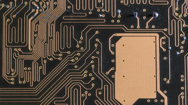
A Fine Line PCB is a printed circuit board engineered with ultra-narrow traces and tight spacing, typically below 100 µm. This enables high-density routing and compact component placement while maintaining excellent signal integrity and reliability. Fine line PCBs are essential in high-speed digital systems, RF modules, 5G devices, IoT equipment, aerospace electronics, and medical instruments.
Importance of Fine Line PCBs
Fine line PCB technology allows engineers to maximize functionality in limited board space, offering:
-
High component density on compact boards
-
Precise signal routing for high-speed digital and RF circuits
-
Improved electrical performance with reduced path lengths
-
Support for advanced IC packages like BGA, QFP, and CSP
These advantages make fine line PCBs indispensable for applications demanding miniaturization, high performance, and reliability.
Challenges in Fine Line PCB Design
Designing fine line PCBs requires overcoming several challenges:
-
Ultra-narrow trace fabrication to avoid shorts and opens
-
Signal integrity management in densely routed boards
-
Thermal management for high-density and high-current circuits
-
Precise manufacturing tolerances to ensure repeatable performance
Key Design and Manufacturing Features
1. Ultra-Fine Trace Technology
-
Trace widths and spacing down to 75 µm or below
-
High-resolution photolithography and laser imaging for precision
2. Controlled Impedance Design
-
Ensures signal integrity in high-speed digital and RF circuits
-
Stack-up and trace routing optimized to minimize crosstalk and loss
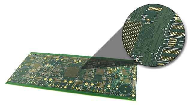
3. Multilayer Fine Line PCB Construction
-
Supports 8 layers or more for complex systems
-
Dedicated power and ground planes for stable voltage and return paths
-
Enables dense routing without compromising reliability
4. Advanced Materials and Surface Finishes
-
Low Dk / low Df laminates, high Tg FR4
-
Surface finishes like ENIG or OSP for improved conductivity and reliability
5. Rigorous Testing and Quality Control
- Automated Optical Inspection (AOI), X-ray, impedance testing, and electrical validation
-
Ensures high yield and reliability for demanding applications
Applications of Fine Line PCBs
-
5G and high-speed communication modules
-
IoT and wearable devices
-
High-speed computing and data center equipment
-
Aerospace and defense electronics
-
Medical devices and precision instrumentation
-
Semiconductor testing and high-density IC boards
Why Choose KKPCB for Fine Line PCB Manufacturing
KKPCB provides comprehensive fine line PCB services, including:
-
Advanced multilayer fine line PCB fabrication
-
Controlled impedance design for high-speed signals
-
Support for ultra-fine traces and high-density IC packages
-
High reliability and yield with strict quality control
-
Engineering support from prototype to mass production
Our team ensures each Fine Line PCB meets the highest standards of performance, reliability, and precision.
