As electronic devices become faster and more complex, maintaining the quality of electrical signals on a PCB is critical. Signal Integrity PCBs are designed to preserve signal quality, minimize noise, and reduce data errors in high-speed circuits. Proper design and manufacturing of these boards are essential for reliable high-performance electronics, from telecommunications and computing to automotive and industrial systems.
What is a Signal Integrity PCB?

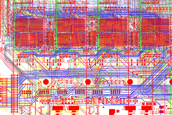
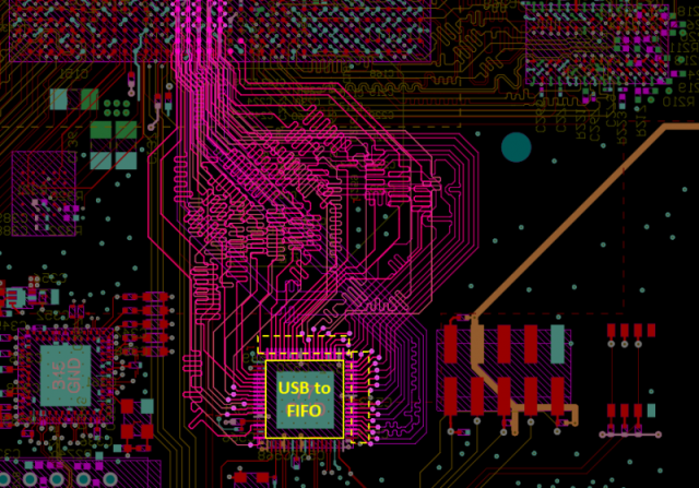
A Signal Integrity PCB is a printed circuit board engineered to maintain the integrity of electrical signals, particularly in high-speed PCB applications. Signal integrity refers to the ability of a PCB to transmit electrical signals without distortion, reflections, crosstalk, or excessive loss. As clock speeds and data rates increase, traditional PCB designs may fail to meet performance requirements, making signal integrity a key focus in modern electronics.
Key Factors Affecting Signal Integrity
-
Trace Impedance
Controlling impedance ensures signals travel consistently with minimal reflections. Microstrip, stripline, and controlled impedance routing techniques are often used in Signal Integrity PCBs. -
Crosstalk Reduction
Closely spaced traces can induce interference. Proper spacing, ground planes, and differential pair routing reduce crosstalk in high-speed designs. -
Material Selection
High-frequency laminates with low dielectric loss (low Df) and stable dielectric constant (low Dk) improve signal integrity. -
Via Design
Minimizing via stubs and using backdrilling techniques prevent signal reflections and loss in HDI PCB designs. -
Power Integrity
Stable and low-noise power delivery is critical for signal integrity. Decoupling capacitors, power planes, and careful layer stack-up are essential. -
Length Matching and Routing
Critical in differential pairs and high-speed buses, ensuring traces are length-matched prevents timing errors and signal skew.
Design Guidelines for Signal Integrity PCBs
-
Use controlled impedance routing for high-speed signals.
-
Maintain proper spacing and shielding to minimize crosstalk.
-
Implement differential pairs for high-speed data transmission.
-
Optimize layer stack-up with dedicated signal, ground, and power planes.
-
Use high-quality PCB materials suitable for high-frequency operation.
-
Apply simulation and modeling tools (like SPICE or HFSS) to verify signal integrity before fabrication.
Applications of Signal Integrity PCBs
-
Telecommunications: High-speed data transmission, routers, and 5G infrastructure.
-
Computing Devices: Servers, CPUs, GPUs, and high-speed memory boards.
-
Automotive Electronics: Advanced driver-assistance systems (ADAS) and infotainment modules.
-
Industrial Systems: High-speed control systems, robotics, and instrumentation.
-
Medical Devices: Precision diagnostic equipment with high-speed digital interfaces.
Conclusion
Signal Integrity PCBs are crucial for high-speed electronics where reliable signal transmission is essential. From impedance control and crosstalk reduction to material selection and via optimization, every design choice impacts performance. Partnering with an experienced PCB manufacturer ensures your Signal Integrity PCB meets the demanding requirements of modern electronics, delivering high-speed, reliable, and efficient performance.
