A High Density PCB (HDPCB) is a printed circuit board designed to support compact, high-performance electronic systems. By leveraging HDI technology, microvias, blind/buried vias, and multilayer stackups, high density PCBs allow engineers to integrate more functionality into smaller footprints, making them essential for smart devices, high-speed computing, RF communication, and semiconductor testing.
Key Features of High Density PCBs
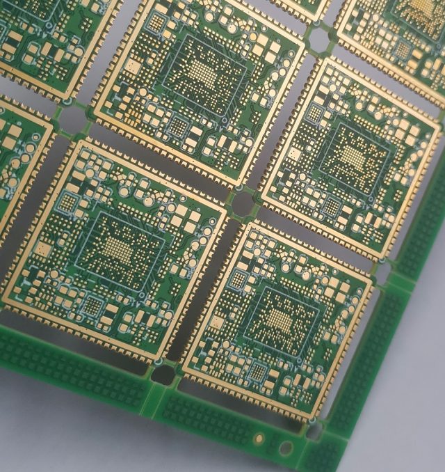
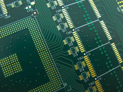
1. High Wiring Density
High density PCBs maximize routing efficiency, enabling fine-pitch BGAs, QFNs, and other high pin count components on a compact board.
2. HDI and Microvia Technology
Using microvias, stacked or staggered via structures, and via-in-pad designs, HDPCBs achieve shorter signal paths, reduced parasitic effects, and superior signal integrity.
3. Multilayer Stackups
Multiple signal, power, and ground layers improve power distribution, EMI suppression, and signal integrity, essential for high-speed or RF circuits.
4. Controlled Impedance Routing
Precise trace width, spacing, and dielectric materials ensure consistent impedance, critical for high-frequency and high-speed signals.
5. Compact Form Factor
HDPCBs reduce board size without compromising performance, ideal for IoT devices, wearable electronics, and automotive modules.
Advantages of High Density PCBs
-
Optimized board space utilization
-
Enhanced signal integrity for high-speed and RF applications
-
Support for fine-pitch, high pin count ICs
-
Improved EMI/EMC performance
-
Better thermal management in compact designs
-
Scalable from prototype to volume production
Applications of High Density PCBs
High density PCBs are widely used in modern electronics, including:
-
Semiconductor IC test and ATE boards
-
High-speed computing and networking equipment
-
5G and RF communication modules
-
Automotive ADAS and ECUs
-
Medical devices and wearable electronics
-
Industrial automation and compact IoT devices
HD PCBs are critical for miniaturization, high performance, and long-term reliability in these applications.
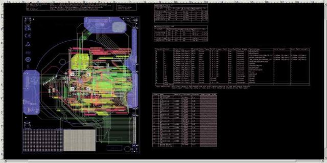
Manufacturing Considerations
Producing high density PCBs requires advanced fabrication and strict quality control:
-
Precise microvia and blind/buried via formation
-
Sequential lamination for multilayer boards
-
High-quality copper plating and surface finish
-
Tight line/space and layer alignment control
-
Electrical testing, AOI, and X-ray inspection for reliability
Experienced manufacturers ensure consistent electrical performance and high yield.
Conclusion
High Density PCBs are the foundation of modern compact and high-performance electronics. Through HDI technology, multilayer stackups, and advanced via structures, HDPCBs provide superior signal integrity, minimized parasitic effects, and reliable performance across applications from IoT and RF to automotive and semiconductor testing.
