As digital systems move toward higher data rates, smaller form factors, and lower power consumption, the demand for High Speed PCB solutions continues to accelerate. From 10–112 Gbps SerDes links to DDR4/DDR5 memory buses and advanced communication modules, a High Speed PCB must deliver loss control, impedance stability, and electromagnetic reliability in increasingly complex environments.
To accomplish this, High Speed PCB engineering requires a precise balance of material science, stackup strategy, and routing discipline, ensuring every signal arrives with minimal distortion or jitter.
1. High-Speed Engineering Context
A High Speed PCB is designed for signals above ~1 Gbps or with edge rates fast enough that transmission-line effects dominate. At this level:
-
Conductor geometry defines impedance
-
Dielectric material defines signal loss
-
Copper roughness defines skin-effect attenuation
-
Layer stackup defines crosstalk and EMI
In high-speed systems, the PCB is no longer a passive carrier—it becomes a fully engineered electrical component.
2. Material Science Driving High Speed PCB Performance
The dielectric substrate determines how a High Speed PCB behaves at high data rates.
Key Material Parameters
• Dielectric Constant (Dk) Uniformity
Lower and stable Dk ensures predictable impedance and reduces propagation delay variation.
• Dissipation Factor (Df / Loss Tangent)
Low Df materials—such as Megtron 6, Isola I-Speed, Panasonic R-5785, Rogers/Hybrid systems—are essential for minimizing insertion loss at multi-GHz frequencies.
• Copper Surface Roughness
Lower roughness = lower conductor loss = cleaner eye diagrams.
• Glass-Weave Effect Mitigation
For high-speed differential pairs, weave-locked laminates prevent skew and phase imbalance.
High Speed PCB reliability begins with selecting the right dielectric system.
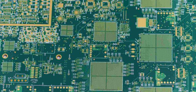
3. High Speed PCB Stackup Engineering
A high-quality stackup ensures electromagnetic consistency and signal integrity.
Critical Stackup Considerations
-
Consistent dielectric thickness for accurate impedance
-
Symmetric stackup to prevent board warpage
-
Dedicated reference planes for return-path stability
-
Low-loss prepregs between high-speed layers
-
Shielding layers to reduce crosstalk and EMI
Engineers often use stripline, dual-stripline, or microstrip structures tailored to specific interface requirements.
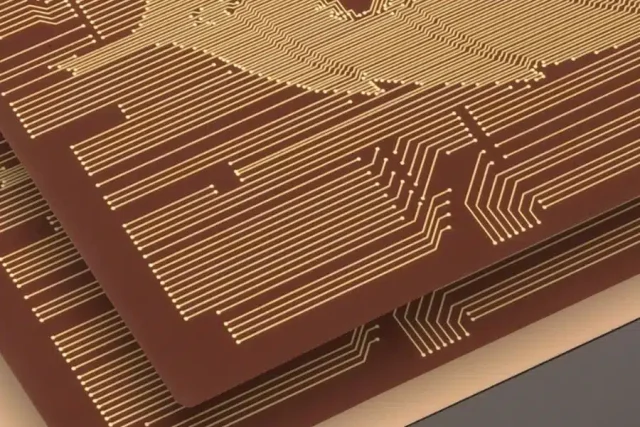
4. High Speed Routing Strategy
For a High Speed PCB, routing is a discipline requiring precision and electromagnetic awareness.
Core High-Speed Routing Techniques
1. Controlled Impedance Lines
Maintaining 50Ω (single) and 85Ω/100Ω (differential) is essential.
2. Differential Pair Management
-
Pair-to-pair spacing
-
Length matching
-
Tight coupling
-
Smooth bends (arc or 45°)
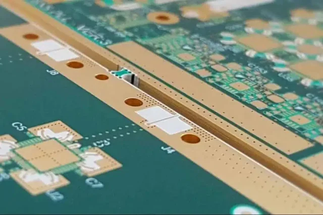
3. Via Optimization
High-speed vias require:
-
Backdrilling
-
Stub removal
-
Anti-pad optimization
-
Low-inductance return vias
4. Crosstalk Minimization
Keep high-speed traces away from noise sources and parallel aggressors.
5. Reference Plane Integrity
Ensure uninterrupted return paths to prevent reflections and mode conversion.
A well-routed High Speed PCB results in clean eye diagrams, lower jitter, and higher data reliability.
5. Manufacturing Precision for High Speed PCB at KKPCB
KKPCB enhances High Speed PCB performance through:
-
Tight dielectric thickness control
-
Low-profile copper foil (HVLP/ROL)
-
Precision LDI imaging for narrow lines
-
High-speed impedance certification
-
Backdrilling capability for via stub removal
-
Low-loss materials stocked for rapid prototyping
-
Automated skew-compensation routing
These capabilities ensure that High Speed PCB designs achieve repeatable, production-grade performance even at very high data rates.
6. Engineering Summary
A High Speed PCB is the foundation of every next-generation digital system. Through advanced materials, optimized stackup, controlled impedance routing, minimized loss, and precise manufacturing, engineers can create PCBs that support:
-
High-speed transceivers (10–112 Gbps)
-
DDR4 / DDR5 memory topologies
-
PCIe Gen4/Gen5
-
High-speed IoT gateways
-
Networking and data-center hardware
With KKPCB’s engineering experience and high-speed fabrication capabilities, High Speed PCB solutions deliver stable, low-jitter, low-loss, and high-reliability performance needed for modern digital applications.
