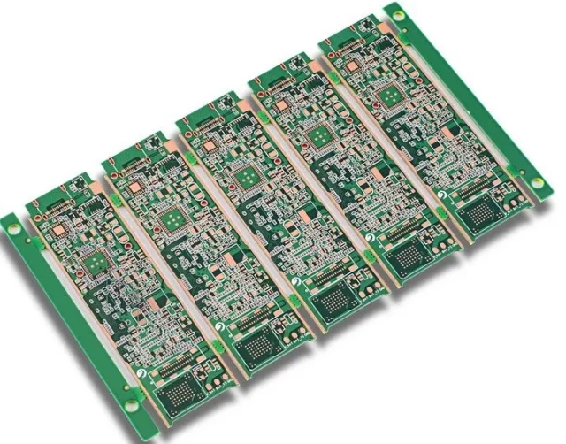
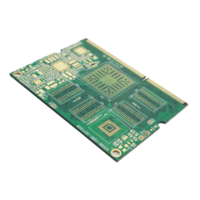
In modern HDI PCB design (High-Density Interconnect PCB design), achieving precise impedance matching is essential for maintaining signal integrity, minimizing reflection, and ensuring high-speed signal transmission. As data rates increase and circuit density grows, impedance control in HDI PCB layout becomes more complex due to fine trace geometries, microvias, and multilayer stack-ups.
Effective impedance matching in HDI PCB design is critical for high-speed digital PCB systems, RF PCB applications, and high-frequency PCB performance.
What Is Impedance Matching in HDI PCB Design?
Impedance matching in PCB design refers to ensuring that the characteristic impedance (Z0) of PCB traces matches the source and load impedance, minimizing signal reflection and power loss.
In HDI PCB design, impedance matching is more challenging due to:
- Ultra-fine trace widths and spacing
- Use of microvias and blind/buried vias
- Complex multilayer PCB stack-up structures
- High component density in HDI PCB layout
Why Impedance Matching Is Critical in HDI PCB Design
Proper controlled impedance in HDI PCB design ensures:
- Reduced signal reflection and return loss
- Improved signal integrity in high-speed PCB routing
- Enhanced RF PCB performance
- Lower EMI and crosstalk
- Stable high-frequency signal transmission
Without proper impedance matching, HDI PCB performance can degrade significantly.
Key Factors Affecting Impedance in HDI PCB Design
1. Trace Geometry (Width, Thickness, Spacing)
Trace dimensions directly determine characteristic impedance in HDI PCB routing.
2. Dielectric Material Properties
The dielectric constant (Dk) and loss tangent affect signal propagation in high-frequency HDI PCBs.
3. PCB Stack-Up Design
Proper HDI multilayer stack-up is essential for consistent impedance.
4. Reference Planes
Stable ground or power planes are required for accurate impedance control PCB design.
5. Via Structures in HDI PCB
Microvias and via transitions introduce impedance discontinuities.
Advanced Impedance Matching Techniques in HDI PCB Design
1. Controlled Impedance Routing
Designing traces with precise width and spacing ensures consistent impedance in HDI PCB layout design.
2. Differential Pair Routing
For high-speed signals, differential impedance control is critical.
Best practices:
- Maintain equal trace lengths
- Control spacing between differential pairs
- Ensure symmetrical routing
3. Microvia Optimization
Microvia design in HDI PCB must minimize parasitic inductance and capacitance.
Techniques:
- Reduce via transitions
- Use stacked or staggered microvias carefully
- Optimize via diameter and pad size
4. Back Drilling and Via Stub Removal
Removing via stubs reduces reflections in high-speed HDI PCB routing.
5. Simulation and Modeling
Using SI (Signal Integrity) simulation tools ensures accurate impedance control.
6. Layer Stack-Up Engineering
Optimized HDI PCB stack-up design ensures stable impedance across layers.
Challenges in Impedance Matching for HDI PCB
- Tight tolerances in fine-line routing
- Manufacturing variations affecting impedance
- Complex via structures in HDI PCBs
- High-frequency signal sensitivity
- Increased crosstalk in dense layouts
Proper DFM (Design for Manufacturing) is essential to overcome these challenges.
Design Guidelines for Impedance Control in HDI PCB
- Use precise impedance calculation tools
- Maintain consistent dielectric thickness
- Avoid abrupt trace width changes
- Minimize discontinuities in routing
- Ensure proper grounding and shielding
- Validate designs using simulation
Applications of HDI PCB Impedance Matching
- High-speed digital systems (DDR, PCIe, USB)
- RF and microwave circuits
- 5G communication devices
- Mobile and wearable electronics
- High-performance computing systems
Advantages of Proper Impedance Matching in HDI PCB Design
- Improved signal integrity and data accuracy
- Reduced EMI and signal reflection
- Enhanced high-frequency PCB performance
- Reliable operation in high-speed systems
- Better overall HDI PCB reliability
Conclusion
Impedance matching in HDI PCB design is a fundamental requirement for achieving high-speed signal integrity and reliable high-frequency performance. By applying advanced techniques such as controlled impedance routing, differential pair design, microvia optimization, and stack-up engineering, engineers can ensure optimal performance in complex HDI PCB systems.
Accurate impedance control, combined with proper simulation and manufacturing considerations, is the key to successful HDI PCB design and high-speed electronics development.
