
Blind and Buried Vias in HDI PCB Design: Engineering Principles, Manufacturing Constraints, and KKPCB’s Advanced Capabilities
As high-density interconnect (HDI) technology becomes essential in 5G, wearables, automotive radar, aerospace, and compact IoT systems, PCB designers increasingly rely on blind vias and buried vias to meet aggressive space, performance, and reliability requirements. These via structures allow designers to escape dense BGA regions, improve signal integrity, and reduce PCB layer count—while enabling compact, high-performance architectures that conventional through-hole vias cannot support.
At KKPCB, our HDI PCB manufacturing capabilities include laser-drilled microvias, stacked and staggered via structures, sequential lamination, resin-filled copper-capped vias, and advanced inspection systems that guarantee structural reliability even in the most demanding environments.
This article provides a rigorous engineering explanation of blind and buried vias, including their definition, design rules, depth limitations, fabrication constraints, and best-use scenarios—told from KKPCB’s manufacturing perspective.
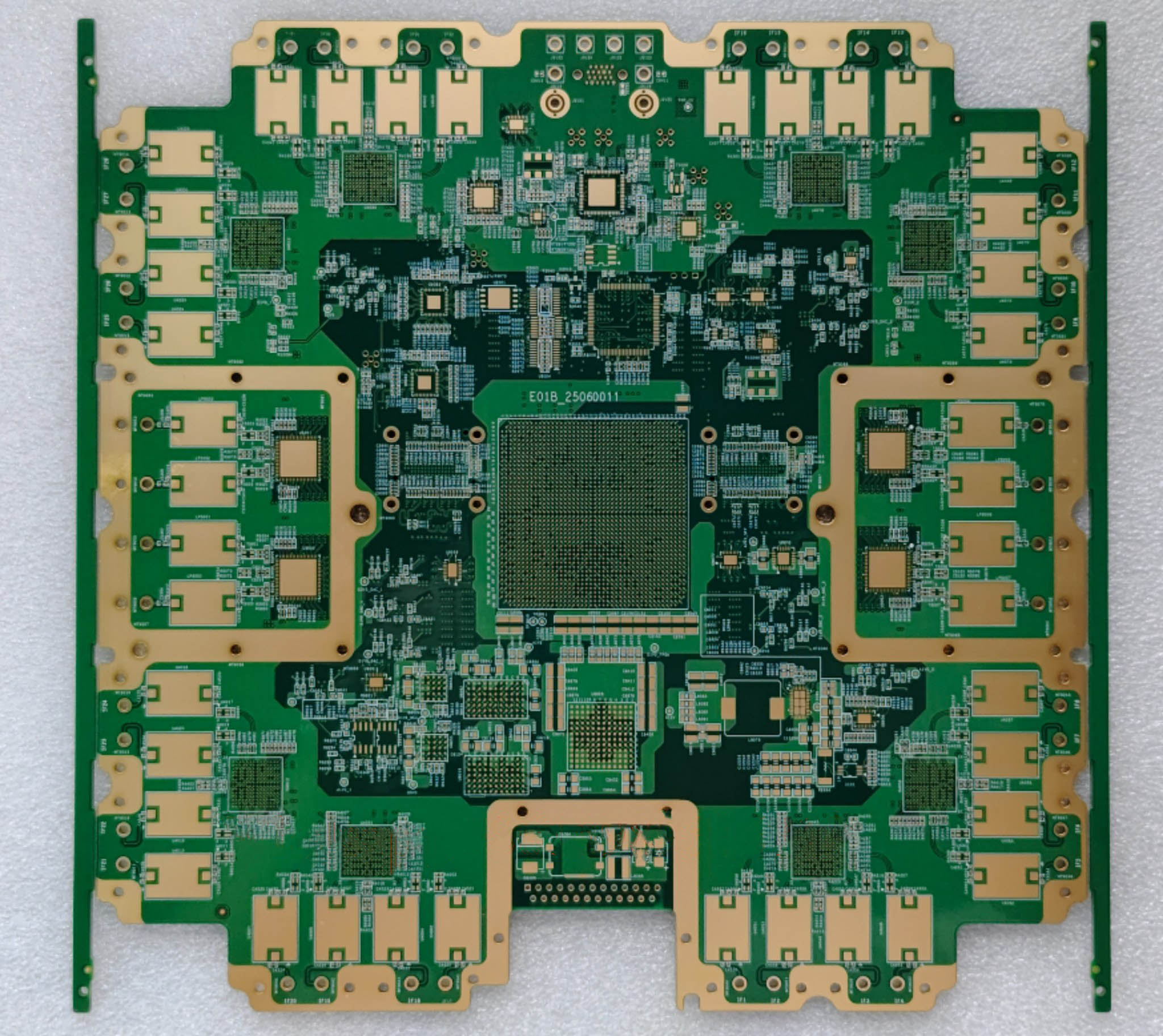
1. What Are Blind and Buried Vias?
Blind Vias
A blind via connects an outer layer of the PCB to one or more inner layers, but does not pass through the entire board.
Used for:
-
HDI escape routing (especially fine-pitch BGAs: 0.4 mm / 0.35 mm / 0.25 mm)
-
Reducing via stubs
-
Improving SI/PI performance
-
Saving routing layers
Buried Vias
A buried via connects inner layers only, and does not reach the outer layers.
Used for:
-
Increasing routing density inside multilayer stack-ups
-
Creating additional space for outer-layer routing
-
Reducing surface clutter for high-speed, RF, and dense analog circuits
Together, these via structures enable compact designs while maintaining signal integrity and manufacturability.
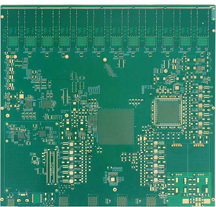
2. Blind vs. Buried Vias: Structural Differences
Feature |
Blind Via |
Buried Via |
|---|---|---|
| Connects | Outer layer → inner layer | Inner layer → inner layer |
| Goes through whole PCB? | No | No |
| Drilling method | Laser or mechanical | Mechanical or laser |
| Typical HDI usage | BGA escape, RF transitions | Inner routing density optimization |
| Fabrication complexity | High | Very high |
| Requires sequential lamination | Yes | Yes |
In HDI manufacturing, blind vias are typically laser-drilled microvias, while buried vias may be mechanical or laser-formed depending on thickness.
3. Engineering Constraints: Critical Rules for Blind & Buried Vias
While they appear simple, blind and buried vias follow strict engineering constraints:
3.1 Vias Must Span an Even Number of Copper Layers
A via cannot start or stop mid-dielectric unless resin-filled and capped.
3.2 Blind Vias Cannot Start at the Bottom Core or End on the Top Core
This is due to:
-
Copper thickness limits
-
Drill-to-copper registration
-
Lamination constraints
3.3 Vias Cannot Intersect or End Inside Another Via
Unless they are:
-
Resin-filled
-
Copper-capped
-
IPC-6012 Class 3 compliant
This process significantly increases cost and must be engineered carefully.
3.4 Depth-to-Diameter Ratio Must Be Controlled
For mechanical drilling:
-
Maximum drill aspect ratio ≈ 6:1 – 8:1
-
Deep blind vias risk:
-
Barrel cracking
-
Poor plating
-
Voids
-
Laser microvias (L1–L2) have a stricter aspect ratio:
-
Depth ≤ 100 µm
-
Diameter: 75–130 µm typical
KKPCB uses advanced LDI + CO₂/UV dual-laser systems for accurate microvia formation.
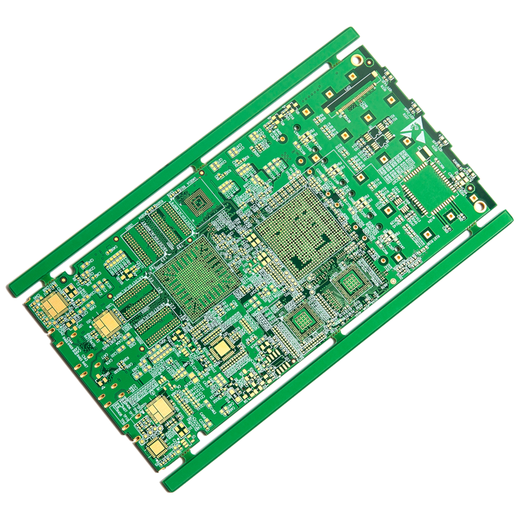
4. Peck Drilling for Blind Vias: Why It Matters
Peck drilling is a controlled drilling method where the drill removes material in multiple small plunges instead of a single deep cut.
Why Peck Drilling Is Critical
-
Prevents drill bit overheating
-
Reduces smear and glass fiber tearing
-
Avoids air pockets that obstruct plating
-
Ensures uniform micro-roughness for reliable copper adhesion
Without proper peck drilling:
-
Via walls become rough or uneven
-
Drill wander increases
-
Plating may not reach the full depth
-
Reliability issues arise (barrel cracks, voids, intermittent connections)
KKPCB engineers apply adaptive peck drilling algorithms based on:
-
Material type
-
Resin content
-
Glass weave style
-
Drill diameter
-
Target depth
This ensures blind vias meet Class 3 reliability standards.
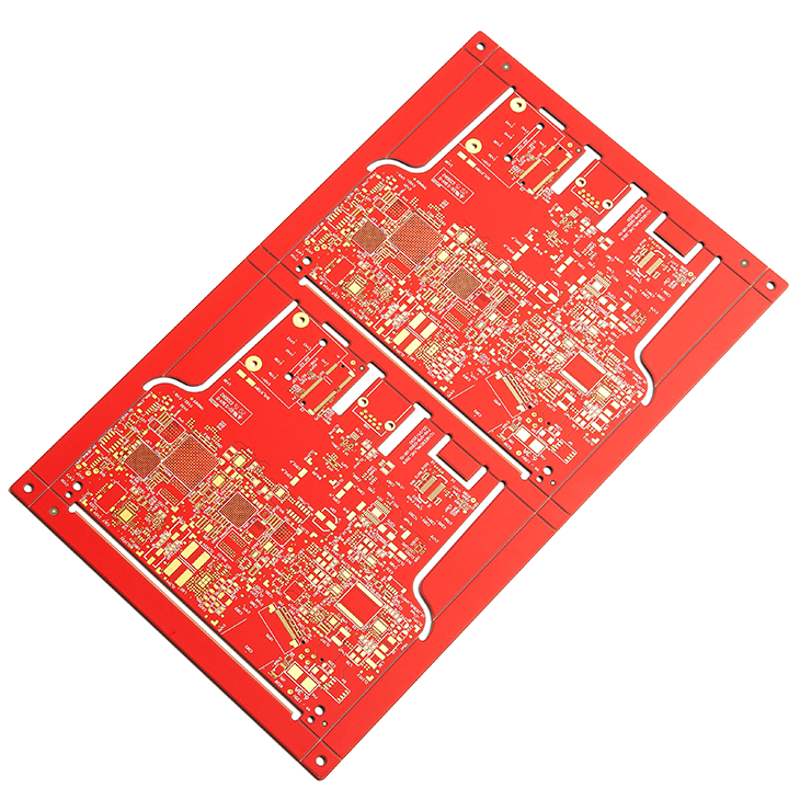
5. Manufacturing Blind & Buried Vias: Sequential Lamination Requirements
Both structures require complex layer-by-layer lamination cycles.
Typical HDI stack-up example:
Each lamination step adds:
-
Cost
-
Processing time
-
Potential for misregistration
KKPCB minimizes these risks using:
-
Automated lamination presses with closed-loop temperature control
-
High-precision laser registration
-
Inline X-ray & AOI inspection
-
Filled-via planarization for stacked structures
6. When Should Designers Use Blind or Buried Vias?
Use Blind Vias When:
-
Escaping ultra-fine BGA pitches (0.4 mm and below)
-
Reducing signal stubs for high-speed (PCIe, SerDes, DDR)
-
Routing RF/microwave transitions with minimized inductance
-
Saving board layers in dense designs
Use Buried Vias When:
-
You need internal routing density
-
The surface must remain clean for:
-
Thermal pads
-
Outer layers must be reserved for critical signals
Use Both for:
-
Smartphones
-
5G RF modules
-
Wearables
-
Radar & ADAS systems
-
Miniaturized medical devices
-
Aerospace/defense electronics
KKPCB routinely supports HDI stack-ups up to 4 sequential lamination cycles with stacked, staggered, and skip-vias.
7. KKPCB’s Advanced Capabilities for Blind & Buried Vias
Manufacturing Technologies
-
UV/CO₂ laser microvia drilling (L1–L2; L2–L3)
-
Resin-filled & copper-capped microvias
-
High-precision mechanical drilling
-
Sequential lamination (HDI 1+n+1, 2+n+2, 3+n+3)
Inspection Technologies
-
AOI for microvia pad land accuracy
-
X-ray for buried via alignment
-
Microsection reliability analysis
-
TDR for impedance integrity
Material Compatibility
Supports:
-
FR-4 High-Tg
-
RCC (Resin-Coated Copper)
-
Polyimide
-
High-frequency PTFE laminates (Rogers/Isola/Taconic)
Conclusion
Blind and buried vias are essential elements in HDI PCB engineering, enabling dense routing, reduced layer counts, superior signal integrity, and compact device form factors. However, they introduce strict mechanical, electrical, and manufacturing constraints that require precision engineering and advanced fabrication techniques.
KKPCB delivers high-reliability blind, buried, and microvia structures through:
-
Advanced drilling technologies
-
Sequential lamination expertise
-
Rigorous reliability testing
-
Engineering-driven DFM guidance
Whether you’re designing next-generation communication modules, RF systems, medical devices, or automotive electronics, KKPCB ensures your HDI architecture meets the highest standards of performance and reliability.
