
With the rapid development of modern electronic systems toward higher communication speeds, higher operating frequencies, and more compact designs, conventional PCB materials such as standard FR-4 are increasingly challenged in high-frequency applications.
A PCB high-frequency board is a specialized printed circuit board designed to transmit signals at high frequencies while maintaining stable electrical performance, low signal loss, and accurate impedance control.
High-frequency PCBs are widely used in applications such as:
- RF communication systems
- Microwave circuits
- Automotive radar
- 5G equipment
- Satellite communication
- High-speed electronic systems
Compared with ordinary PCBs, high-frequency boards require stricter control of:
- Dielectric properties
- Signal integrity
- Material characteristics
- Manufacturing precision
1. Definition of PCB High-Frequency Board
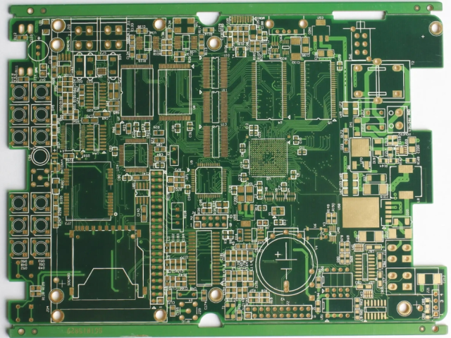
A high-frequency PCB refers to a circuit board designed for electronic circuits operating in high-frequency ranges, generally involving frequencies from hundreds of MHz to GHz levels.
In these applications, signals behave differently from low-frequency electrical currents. Transmission characteristics are affected by:
- Electromagnetic fields
- Transmission line structures
- Dielectric materials
- Surface conditions
Therefore, high-frequency PCB design focuses not only on circuit connectivity but also on maintaining predictable signal transmission performance.
2. Differences Between High-Frequency PCB and Conventional PCB
2.1 Material Difference
Traditional PCBs commonly use:
- FR-4 epoxy laminate
High-frequency PCBs often use specialized materials such as:
- PTFE-based laminates
- Rogers high-frequency materials
- Ceramic-filled materials
- Low-loss resin systems
These materials provide better control of:
- Dielectric constant (Dk)
- Dissipation factor (Df)
- Signal attenuation
2.2 Electrical Performance Difference
High-frequency PCBs require:
Low Dielectric Loss
A low dissipation factor reduces energy loss during signal transmission.
This helps improve:
- Signal strength
- Transmission efficiency
- System reliability
Stable Dielectric Constant
The dielectric constant affects signal propagation speed and impedance.
A stable Dk helps maintain:
- Accurate impedance
- Consistent electrical performance
2.3 Manufacturing Precision Difference
High-frequency boards require tighter manufacturing control.
Important parameters include:
- Copper thickness tolerance
- Dielectric thickness tolerance
- Trace width accuracy
- Surface roughness
- Layer alignment
Small variations can affect RF performance.
3. Key Characteristics of High-Frequency PCB Materials
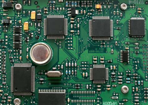
3.1 Low Dielectric Constant (Dk)
The dielectric constant determines how signals travel through the PCB material.
A stable Dk helps:
- Maintain signal timing
- Improve impedance control
- Reduce design variation
3.2 Low Dissipation Factor (Df)
The dissipation factor represents dielectric energy loss.
Lower Df provides:
- Lower insertion loss
- Better high-frequency efficiency
3.3 Low Signal Attenuation
High-frequency materials reduce:
- Transmission loss
- Signal degradation
This is especially important for:
- Microwave circuits
- High-speed communication systems
3.4 Good Thermal Stability
High-frequency boards often operate under demanding conditions.
Good thermal stability helps maintain:
- Electrical consistency
- Mechanical reliability
4. Common High-Frequency PCB Materials
4.1 Rogers PCB Materials
Rogers materials are widely used for RF and microwave applications.
Common materials include:
- RO4003C
- RO4350B
- RO4835
- RT/Duroid series
Advantages:
- Stable dielectric properties
- Low loss performance
- Reliable high-frequency operation
Applications:
- RF modules
- Antenna boards
- Radar systems
4.2 PTFE-Based Materials
PTFE materials provide excellent high-frequency characteristics.
Advantages:
- Extremely low dielectric loss
- Excellent phase stability
Applications:
- Microwave circuits
- Aerospace communication systems
Challenges:
- More complex processing
- Higher manufacturing requirements
4.3 Ceramic-Based Materials
Ceramic substrates provide:
- High thermal conductivity
- Excellent electrical performance
- High-temperature resistance
Applications:
- Power RF devices
- High-reliability electronics
5. Design Considerations for High-Frequency PCB
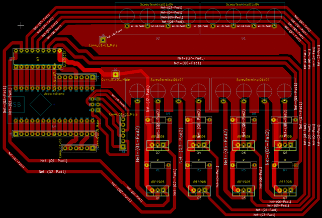
5.1 Impedance Control
Impedance control is one of the most important aspects of high-frequency PCB design.
Common requirements include:
- 50Ω single-ended impedance
- 100Ω differential impedance
Factors affecting impedance:
- Trace width
- Copper thickness
- Dielectric thickness
- Material Dk
Manufacturing verification may use:
- TDR testing
- Impedance coupons
5.2 Transmission Line Design
High-frequency signals should be routed using controlled transmission structures.
Common structures include:
Microstrip
A signal trace placed above a reference plane.
Advantages:
- Simple structure
- Easy fabrication
Stripline
A signal trace embedded between reference planes.
Advantages:
- Better electromagnetic shielding
- Stable impedance performance
5.3 Grounding Design
A proper grounding structure is essential.
Good grounding helps:
- Reduce EMI
- Improve signal return paths
- Prevent noise coupling
Common methods include:
- Continuous ground planes
- Ground via stitching
- Proper RF area isolation
5.4 Signal Path Optimization
High-frequency routing should:
- Minimize trace length
- Avoid unnecessary vias
- Reduce sharp corners
- Maintain consistent geometry
These methods reduce:
- Signal reflection
- Insertion loss
- Electromagnetic interference
6. Manufacturing Requirements for High-Frequency PCB
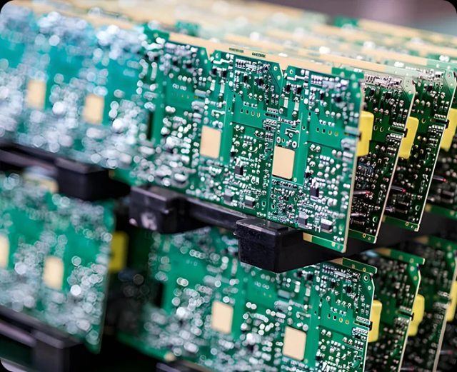
6.1 Material Processing Control
Manufacturing must control:
- Lamination temperature
- Resin flow
- Layer alignment
Incorrect processing may affect:
- Dielectric thickness
- Impedance accuracy
6.2 Copper Surface Control
At high frequencies, current flows mainly near the conductor surface due to the skin effect.
Copper roughness can increase:
- Conductor loss
- Signal attenuation
Therefore, low-profile copper foil is often preferred.
6.3 Surface Finish Selection
Surface finishes should consider:
- Electrical performance
- Reliability
- Assembly requirements
Common finishes:
- ENIG
- ENEPIG
7. Applications of High-Frequency PCB
7.1 RF Communication Systems
Applications:
- Wireless modules
- Base stations
- 5G communication equipment
Requirements:
- Low signal loss
- Stable impedance
7.2 Automotive Radar Systems
Applications:
- 24GHz radar
- 77GHz radar
Requirements:
- High-frequency stability
- Precise signal transmission
7.3 Aerospace and Satellite Electronics
Applications:
- Satellite communication
- Navigation systems
Requirements:
- High reliability
- Phase stability
7.4 IoT and Wireless Devices
Applications:
- Smart sensors
- Connected devices
Requirements:
- Compact size
- Reliable RF performance
8. Advantages and Challenges of High-Frequency PCB
Advantages
- Excellent high-speed signal transmission
- Low insertion loss
- Stable impedance performance
- Suitable for GHz applications
- Improved RF system reliability
Challenges
- Higher material cost
- More complex manufacturing process
- Requires advanced PCB fabrication capability
- Greater sensitivity to process variation
9. Future Development Trends
As electronic systems continue advancing toward:
- Higher frequency bands
- Faster data transmission
- More integrated RF functions
high-frequency PCBs will continue evolving.
Future trends include:
Higher Frequency Applications
Examples:
- mmWave communication
- Advanced radar systems
Low-Loss Material Development
Future materials will focus on:
- Lower dielectric loss
- Better thermal stability
- Improved signal integrity
Advanced Manufacturing Technology
Development directions include:
- More precise impedance control
- Improved surface treatment
- Advanced multilayer structures
Conclusion
A PCB high-frequency board is a specialized circuit board designed to support reliable signal transmission in high-frequency electronic systems.
Its performance depends on:
- Appropriate material selection
- Controlled impedance design
- Optimized routing
- Proper grounding
- Precise manufacturing processes
Compared with conventional PCBs, high-frequency boards provide superior electrical performance and are essential for modern technologies such as 5G communication, automotive radar, microwave systems, and high-speed electronic equipment.
