Introduction: Why SiC PCB Matters in the New Era of Power Electronics
Silicon Carbide (SiC) power devices are redefining the performance limits of modern power electronics. To unlock the true efficiency of SiC MOSFETs, SiC diodes, and SiC power modules, engineers require PCB platforms that can handle extreme thermal loads, high switching frequencies, and elevated voltages.
This is where the SiC PCB becomes mission-critical. A well-engineered SiC PCB enables efficient heat dissipation, stable dielectric performance, and reliable power cycling—directly impacting system longevity and efficiency.
1. Material Engineering Behind SiC PCB Technology
The foundation of a high-performance SiC PCB lies in its substrate:
Common Substrates for SiC PCB
-
Aluminum Nitride (AlN) – Best match for SiC due to 170–240 W/m·K thermal conductivity
-
Aluminum Oxide (Al₂O₃) – Economical alternative with moderate thermal performance
-
DBC / DPC Ceramic Structures – Direct bond copper ideal for high-power SiC modules
-
Metal-Core SiC PCB – Useful for distributed cooling in power conversion systems
A SiC PCB must maintain structural stability under extreme temperatures (150–300°C) and withstand high-dV/dt switching common in SiC devices.
2. Thermal Management: The Most Critical Factor in SiC PCB Design
SiC devices generate intense heat due to high power density.
A SiC PCB optimizes thermal spreading through:
-
Ceramic substrates with ultra-low thermal resistance
-
Thick copper layers (2–12 oz) for heat spreading
-
Thermal vias or filled microvias connecting heat paths
-
Embedded copper coins beneath SiC MOSFETs
Advanced thermal modeling shows that a well-designed SiC PCB can reduce junction temperature by up to 30–45°C, directly extending device lifespan.
3. Electrical Performance Requirements for SiC PCB
High-speed switching of SiC devices (up to 100–500 kHz) demands exceptional electrical design:
Key electrical constraints of SiC PCB:
-
Low inductance loop design for gate and power loops
-
Controlled impedance traces to prevent overshoot and ringing
-
Optimized ground reference planes for high-frequency SiC switching
-
Shortened Kelvin-source connections for accurate switching control
Every nanohenry of stray inductance in a SiC PCB can significantly deform high-speed switching waveforms.
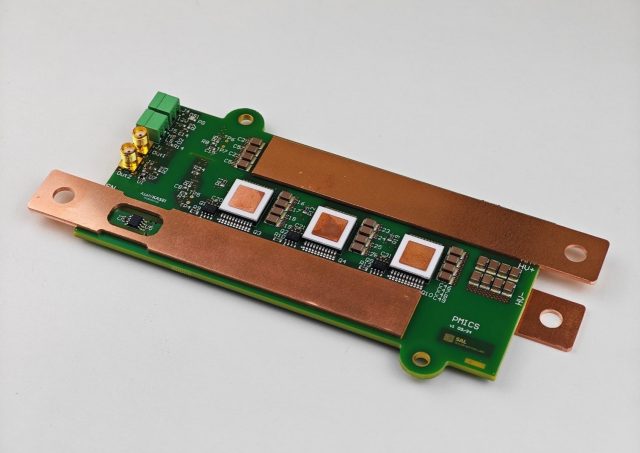
4. High-Voltage Isolation & Dielectric Reliability
A high-performance SiC PCB must withstand repetitive high-voltage transients:
-
Isolation requirements: 2 kV – 10 kV
-
CTI rating: ≥ 600
-
Creepage & clearance rules: aligned with IEC 60664
-
Multi-layer ceramic insulation for high reliability
These characteristics make SiC PCB suitable for EV inverters, industrial drives, renewable-energy converters, and aerospace power modules.
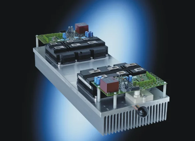
5. Application Scenarios Where SiC PCB Is Transformative
SiC PCB is widely used in:
-
EV traction inverters
-
Onboard chargers (OBC)
-
Solar inverters & energy storage systems
-
High-frequency power supplies
-
Motor drives & robotics power modules
-
High-power RF and microwave systems
-
Aerospace electrical systems
Whenever extreme efficiency and thermal performance are required, SiC PCB becomes the optimal solution.
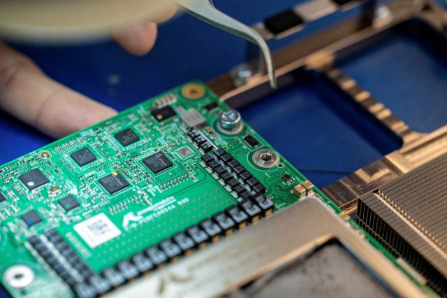
6. Why KKPCB Excels in SiC PCB Manufacturing
KKPCB provides engineering-grade SiC PCB manufacturing with:
-
AlN / Al₂O₃ ceramic SiC PCB fabrication
-
DBC / DPC technologies for power modules
-
High-thickness copper (up to 12 oz)
-
IPC-Class 3 reliability
-
Full engineering support from stackup to thermal simulation
Our process ensures optimized heat dissipation, voltage isolation, and electrical performance tailored for SiC applications.
Conclusion
As power electronics accelerate toward higher efficiency and compactness, SiC PCB technology becomes indispensable. The unique combination of thermal conductivity, high-voltage endurance, and wide-bandgap compatibility makes SiC PCB an essential platform for next-generation power systems.
For companies pursuing world-class power electronics, partnering with an expert SiC PCB manufacturer is a strategic advantage.
