
Table of Contents
- Feed field boundary
- Ground and shield continuity
- Connector and assembly access
- Manufacturing release
Compact wireless modules rarely fail because the antenna feed is absent from the layout. They fail because the feed keep-out is treated as empty space instead of a controlled electromagnetic and manufacturing feature. A Taconic RF-35 PCB can provide a stable RF platform, but only when copper, vias, shield frames, connector hardware, and assembly access are released as one geometry.
Define the Taconic RF-35 PCB feed keep-out as a field boundary
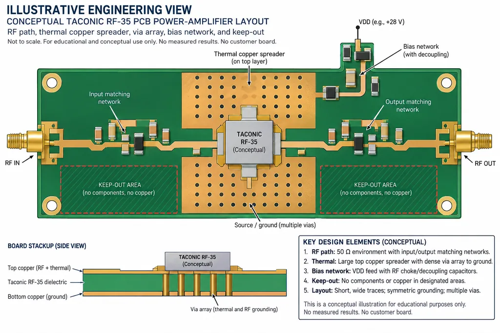
The keep-out around a Taconic RF-35 PCB antenna feed controls where the return current can flow and where nearby copper can disturb the field. Start with the feed type—microstrip, coplanar waveguide, or a transition through the stackup—and draw the reference-plane boundary around it. The boundary should cover the feed, its first bend, the launch pad, and the ground transition, not only the visible antenna trace.
For a Taconic RF-35 PCB, record the layer, dielectric height, trace width, side-ground spacing, via-fence rule, and solder-mask condition in the design notes. If the antenna is tuned with a matching network, keep the component pads and ground returns inside the same review zone. This makes a layout change auditable when the module is repackaged.
| Keep-out element | Why the project team cares | DFM check |
|---|---|---|
| Feed trace | Controls impedance and phase through the launch | Finished width and corner rule |
| Reference plane | Sets the return-current path | No unintended splits or slots |
| Ground fence | Limits coupling into nearby circuits | Pitch, drill, and annular-ring review |
| Shield frame | Changes the field boundary and assembly access | Frame-to-feed clearance and solder-mask opening |
Keep ground and shield boundaries continuous
Ground pour on a Taconic RF-35 PCB is not automatically a good RF ground. A copper island beside the feed can add capacitance without providing a low-inductance return. A shield can improve isolation while also narrowing assembly access or forcing a new via pattern. Review the complete boundary in plan view and cross-section.
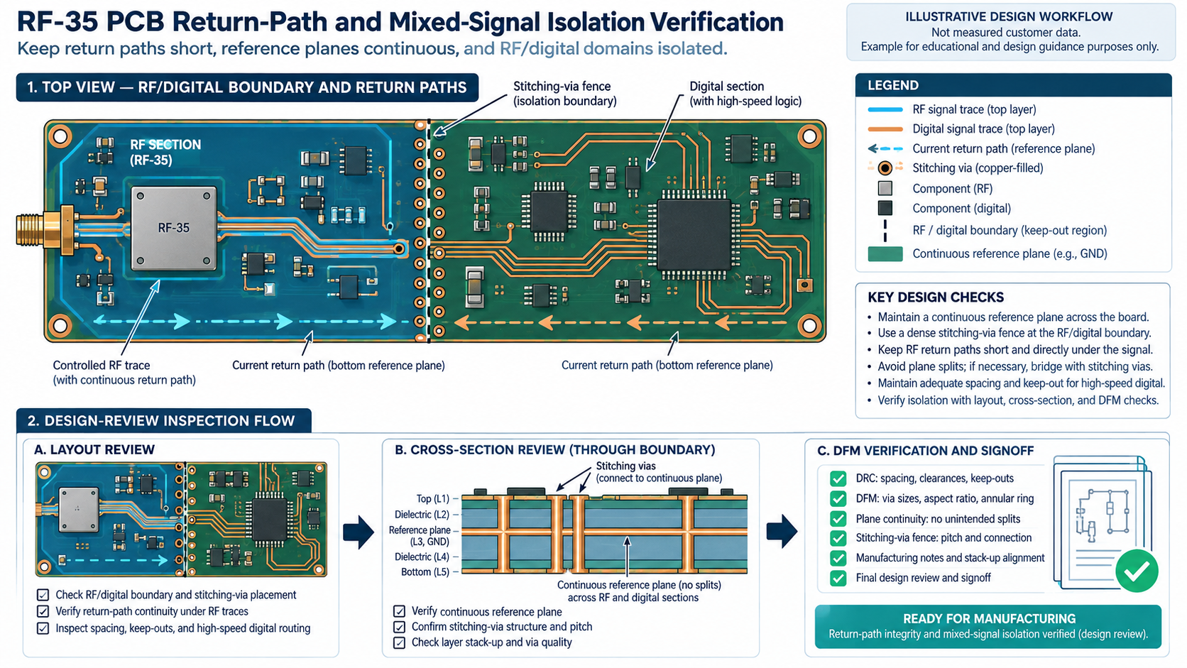
When the feed crosses layers, use a via transition that preserves the reference plane. A PCB design review should mark every plane change, slot, mounting hole, and shield opening that intersects the return path. If a keep-out removes ground vias, the model must be rerun rather than accepted as a cosmetic clearance.
For dense radio modules, place sensitive digital clocks and switching nodes outside the feed boundary. If that is impossible, add a defined shield or stitching strategy instead of relying on a late copper pour. The goal is a repeatable electromagnetic boundary that the CAM team can see in the fabrication data.
Coordinate connector, antenna, and assembly access
Connector launches on a Taconic RF-35 PCB and antenna feeds often share the same edge region. Leave room for the connector body, torque tool, solder fillet, inspection camera, and rework nozzle. A keep-out that is electrically correct but mechanically inaccessible becomes a schedule risk during pilot assembly.
Use the same datum for the connector, antenna edge, and module shield. The Taconic RF-35 PCB drawing should identify which dimensions are RF-critical and which are mechanical reference dimensions. That separation helps the project manager control a housing change without allowing a non-critical enclosure tolerance to move the feed.
Release keep-outs that manufacturing can inspect
A Taconic RF-35 PCB keep-out should be visible in the fabrication drawing, not only in an engineer’s layout layer. Add a layer-by-layer map for the feed, shield, ground fence, solder-mask opening, and component courtyard. Identify any region where a via is intentionally omitted and explain the reason.
KKPCB’s PCB manufacturing handoff can check registration between the feed, mask, and shield frame. It can also review whether the via drill, copper spacing, and panelization leave enough process margin. If the design uses controlled impedance, link the feed class to the stackup and coupon rather than leaving the fabricator to infer it.
Make the antenna keep-out a project decision
Before release, the team should answer four questions: Is the feed boundary defined in every copper layer? Is the return path continuous through each transition? Can assembly and inspection reach the connector and shield? Does the coupon represent the most sensitive geometry? Those answers create a practical PCB assembly and DFM gate.
A compact Taconic RF-35 PCB module is easier to tune and easier to build when keep-outs are treated as controlled geometry. The result is fewer late copper edits, clearer responsibility between design and manufacturing, and a more predictable path from antenna prototype to repeatable production.
A second Taconic RF-35 PCB review should confirm that the final keep-out matches the released material and stackup. Pair it with an RF keep-out checklist and a wireless module PCB mechanical datum.
Sources: public RF-35 material data; Analog Devices RF layout guidance on reference planes and return paths; KKPCB DFM, fabrication, and assembly workflow information reviewed for this article.
