
A connected door controller, smart thermostat, or appliance gateway may combine a mains input with a low-voltage sensor and a radio module on one compact board. The difficult project decision is not whether a relay can switch; it is whether the board, enclosure, assembly process, and verification fixture preserve the isolation boundary when the product moves from prototype to production. This article explains how to release a Smart Home PCB with explicit creepage, clearance, slot, and test access.
- Partition mains, isolated power, radio, and sensor zones before routing.
- Use slots, barriers, and component placement to protect the intended insulation path.
- Keep coating, mounting, and connector decisions from bridging the boundary.
- Release safety checks with the same board and fixture revision.
Define the electrical boundary before choosing the stackup
Start with the product voltage class, pollution environment, enclosure material, and connector exposure. The board outline and mounting bosses can create a shorter path than the routed copper. A PCB design review should therefore draw the high-energy side, the isolated low-voltage side, and every crossing point for power, signal, shield, or mounting hardware. A Smart Home PCB material choice must support the intended insulation system, but a material name alone does not prove the complete product path.
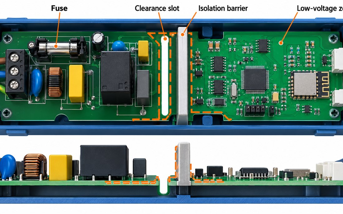
Use a physical barrier or slot when the enclosure, contamination level, or component body makes a surface path uncertain. The PCB manufacturing drawing should call out slot width, edge treatment, copper pull-back, and any allowed routable region. Do not hide those controls in a net-class rule that the assembly and inspection teams cannot see.
Keep copper, hardware, and coating from bridging the boundary
A copper pour may stop at the correct line while a mounting washer, shield spring, probe pin, or coating meniscus crosses it. The PCB assembly package should show component body limits, keep-out zones, and the hardware datum. If a connector or cable shield approaches the barrier, document whether it belongs to protective earth, chassis, signal return, or the isolated domain. The RF PCB return path must remain intentional without turning a shield into an accidental bridge.
| Boundary feature | Project question | Release evidence |
|---|---|---|
| Clearance | Is the shortest air path visible after assembly? | Layout overlay and inspection photo |
| Creepage | Does the surface path avoid slots, residue, and hardware? | Drawing note and material record |
| Isolation slot | Will routing and depanelization preserve the slot? | Drill file and first-article check |
| Coating mask | Can the coating stop without wicking across the boundary? | Mask artwork and process traveler |
Design the verification fixture with safe access
A production check is credible only when operators can connect the guarded input, the low-voltage output, and the reference instrument without improvising. The assembly fixture should provide a mechanical datum, protected probe access, and a connector key that cannot be reversed. The PCB materials and coating instructions must be visible in the same traveler because residue or an approved substitute can change the surface path.
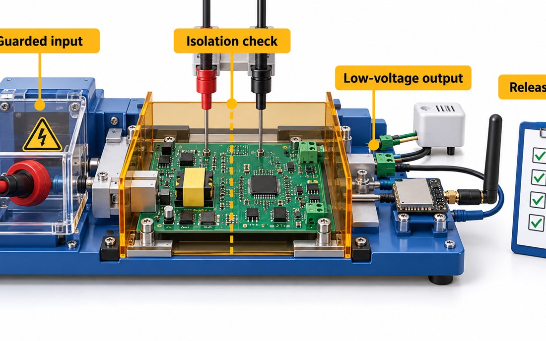
Do not present a fixture screenshot as a certification report. Record the instrument identity, board revision, fixture revision, and acceptance method, then distinguish a design target from a measured production result. The PCB fabrication traveler should preserve the same identifiers through panel separation, cleaning, coating, and final inspection.
Release checklist for an isolated smart-home board
- Overlay the isolation boundary on copper, drill, assembly, and enclosure drawings.
- Check the shortest path after connector, fuse, relay, shield, and mounting hardware are installed.
- Verify slot and edge treatment after depanelization.
- Confirm coating masks and cleaning instructions cannot create a conductive bridge.
- Repeat the controlled verification sequence after any power, relay, enclosure, or connector ECO.
The final Smart Home PCB release should make the boundary easy to see and hard to misinterpret. When engineering, manufacturing, assembly, and procurement use the same barrier drawing, a late component substitution becomes a controlled decision. The isolation layout remains connected to the fabrication note, the assembly traveler, and the material approval.
The Smart Home PCB stackup must be released with the boundary drawing, and the Smart Home PCB layout must retain the same datum after an ECO.
For project managers, the practical handoff is a single release package: board files, stackup, barrier drawing, component and coating notes, fixture method, and change history. That package lets a factory ask a precise question before build rather than discovering an isolation ambiguity after a failed sample.
The release owner should connect the power integrity note to the isolation review.
One isolation record for every Smart Home PCB change
When a Smart Home PCB moves into pilot production, the Smart Home PCB owner should compare the barrier overlay with the enclosure and connector drawings. A Smart Home PCB coating instruction must name the masked surfaces and the approved cure condition. If a Smart Home PCB relay or fuse changes, the fixture datum and guarded input need a fresh review. If a Smart Home PCB radio module changes, the return path and shield interface must be checked without crossing the barrier. The Smart Home PCB release package is complete only when those decisions, the board revision, and the fixture revision agree.
The Smart Home PCB inspection photo should show the boundary after assembly, and the Smart Home PCB traveler should retain the acceptance method without implying a certification result.
This makes the Smart Home PCB release auditable from the enclosure boundary to the final production record.
The Smart Home PCB board outline, the Smart Home PCB barrier, and the Smart Home PCB fixture datum should share one controlled revision. That gives the Smart Home PCB team a clear answer when procurement asks whether a substitute component changes the Smart Home PCB isolation path.
Sources: Analog Devices isolation and mixed-signal design guidance; Würth Elektronik PCB assembly and EMC notes; Qorvo RF integration references; connector, relay, coating, insulation, and PCB material supplier application data. The workflow above is a design and release method, not a customer certification result.
