
An industrial sensor gateway can appear simple on a block diagram: a 24 V field cable, a converter, an analog input, and a network link. In service, that cable carries switching noise, surge energy, shield current, and ground-potential differences that the block diagram hides. A reliable Industrial IoT PCB release begins by separating the field problem from the quiet measurement problem, then proving that the boundary survives assembly and enclosure integration.
- Define the field connector, shield datum, and surge path before routing.
- Keep converter and protection current away from analog reference paths.
- Use the stackup and copper balance to support a repeatable return path.
- Release a fixture that records noise, thermal state, and board revision together.
Partition the 24 V entry before the schematic becomes copper
Place the field connector, fuse or resettable protector, surge clamp, and chassis or shield landing as one entry zone. The PCB design should show where the high-current transient returns before it reaches the isolated converter. A long trace between the connector and clamp can create a voltage gradient that looks like an analog error later. The Industrial IoT PCB material choice matters, but the first decision is geometric: keep the dirty field loop compact and keep it out of the sensor reference region.
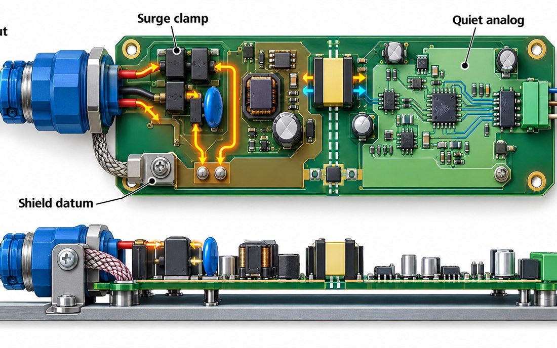
A shield is not automatically signal ground. Decide whether it bonds at the connector, chassis, or a controlled transition, and put that decision in the PCB manufacturing drawing so the operator can see the intended hardware. If the cable enters a metal cabinet, the mounting hardware and washer stack can become part of the return path. Treat those parts as design features rather than procurement details.
Give the analog channel a quiet reference
Keep sensor excitation, ADC reference, and low-level return currents away from the converter switch node and relay or motor outputs. A controlled-impedance PCB rule may be needed for a network or clock path, but it does not replace a clean analog return. Use a clear split strategy, a deliberate bridge point where required, and a test pad that can be probed without lifting a component.
| Zone | Primary risk | Release check |
|---|---|---|
| Field entry | Surge and shield current | Clamp placement and chassis datum |
| Power conversion | Switch-node coupling | Loop geometry and thermal clearance |
| Analog front end | Reference movement | Probe access and return-path review |
| Network edge | Cable emission or radiated pickup | Connector, shield, and stackup overlay |
The PCB assembly drawing should identify polarity, high-voltage or field-side keep-outs, and the order of shield hardware installation. A component substitution that changes package height or heat flow can move the quiet reference even when the netlist is unchanged.
Use the enclosure and stackup as part of the noise design
Industrial cabinets add cable shields, DIN-rail metal, mounting screws, and airflow. The PCB materials, copper weight, and layer reference should be released with the mechanical datum. If the network edge uses a fast differential pair, keep the reference plane continuous through the connector transition and avoid forcing the pair around a shield screw. If the analog channel is slow, prioritize return-current containment and field-loop separation over cosmetic symmetry.
Document a stackup that the PCB fabrication supplier can hold. A nominal dielectric thickness is not enough when the board uses controlled impedance, thermal copper, and isolation slots in the same area. The project manager should receive the stackup, drill table, copper balance note, and approved substitute list as one release package.
Make validation repeatable at the production boundary
Use a test setup that can apply a representative field stimulus, monitor the analog reference, observe a network or clock node, and record a thermal probe position. The assembly fixture needs a board datum and connector key so the cable shield is not left to operator interpretation. A conceptual setup is shown below; it is a workflow aid, not a customer measurement.
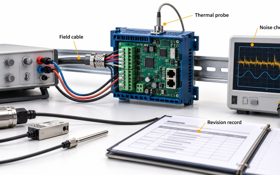
Record board revision, fixture revision, cable length, stimulus profile, and acceptance method. Do not label a design target as a measured result. The DFM review is complete only when probe access, panel separation, and connector strain are included. The manufacturing traveler should keep those checks with the board lot.
Release checklist for an Industrial IoT PCB
- Trace the 24 V surge loop from connector to clamp and chassis.
- Review analog return, converter switch node, and shield datum on one overlay.
- Confirm stackup, copper weight, and connector launch assumptions.
- Check fixture datum, cable keying, probe access, and thermal probe location.
- Repeat the release review after a connector, enclosure, or protection-device ECO.
A production-ready Industrial IoT PCB makes field energy, quiet measurement, and manufacturing evidence visible to the same team. When those interfaces are controlled, a noisy cabinet becomes a solvable engineering problem rather than a late system-integration surprise.
The procurement handoff should name the approved laminate, assembly finish, and signal-integrity rule. The fabrication release then has a defensible basis for the next lot.
The Industrial IoT PCB stackup should stay with the field-entry drawing, and the Industrial IoT PCB layout should preserve the same shield datum after an ECO.
Freeze the field interface at pilot release
When an Industrial IoT PCB enters pilot build, the Industrial IoT PCB owner should compare the field connector, shield datum, and surge path with the enclosure. If an Industrial IoT PCB changes its converter or protection device, repeat the cable and analog-reference review. An Industrial IoT PCB stackup change can move the quiet return even when the schematic is identical. The Industrial IoT PCB fixture should identify cable length and probe datum. That makes an Industrial IoT PCB noise complaint traceable to a board, cable, or fixture revision.
The Industrial IoT PCB release record should distinguish a design target from a measured production result. The Industrial IoT PCB traveler should keep the same cable, fixture, and board identifiers.
Sources: Analog Devices mixed-signal and power-integrity guidance; Würth Elektronik EMC, grounding, and assembly notes; Qorvo interface references; connector, surge-protection, converter, sensor, and PCB material supplier application data. Values above are engineering practices or design targets, not customer measurements.
