What Is an RO4003C PCB?
An RO4003C PCB is a high-frequency printed circuit board manufactured using Rogers RO4003C laminate, specifically designed for RF, microwave, and high-speed digital applications. RO4003C combines low dielectric loss, tight dielectric constant control, and good thermal stability, making it a popular and cost-effective alternative to PTFE-based materials.
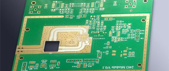
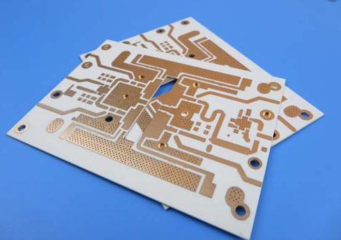
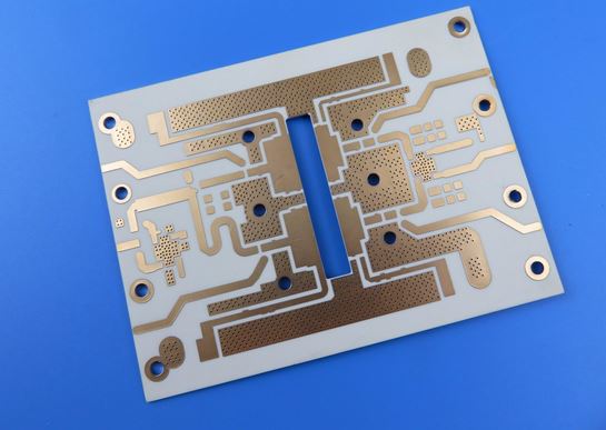
RO4003C PCBs are widely used in 5G communication modules, RF front-end circuits, antennas, wireless networking equipment, and automotive electronics.
Key Advantages of RO4003C PCB
RO4003C material offers several benefits compared with standard FR-4 and some PTFE laminates:
-
Low dielectric loss (Df ~0.0027 @ 10 GHz)
-
Stable dielectric constant (Dk ~3.38) across frequency
-
Excellent impedance control accuracy
-
Good thermal stability and low Z-axis expansion
-
FR-4-like processing, reducing manufacturing cost
These advantages make RO4003C PCB ideal for high-frequency signal transmission with cost efficiency.
RO4003C vs FR-4
Compared with conventional FR-4 materials, RO4003C PCBs provide:
-
Lower signal attenuation at high frequencies
-
Better signal integrity and reduced insertion loss
-
More consistent impedance control for RF traces
-
Improved performance in 5G and microwave applications
This makes RO4003C the preferred choice for RF and microwave designs beyond the capability of standard FR-4.
Key Design Considerations for RO4003C PCBs
1. Controlled Impedance Design
RO4003C is ideal for microstrip and stripline RF traces. Accurate stack-up planning and trace geometry ensure consistent characteristic impedance.
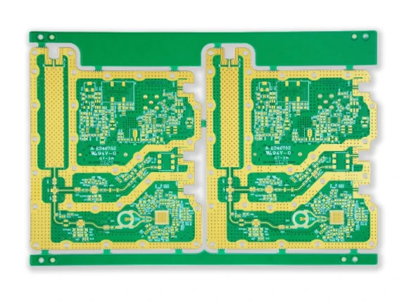
2. Hybrid Stack-Up with FR-4
RO4003C is often combined with FR-4 in multilayer designs to reduce cost while maintaining high-frequency performance. Proper lamination and CTE management are critical.
3. RF Trace Routing
Short signal paths, smooth trace transitions, and proper grounding minimize reflections and EMI.
4. Via and Grounding Strategy
Optimized via placement and stitching vias improve return paths and RF performance.
5. Manufacturing Precision
Tight etching tolerances and process control are essential to preserve electrical consistency in RO4003C PCBs.
Applications of RO4003C PCB
-
5G RF modules and antennas
-
RF front-end and power amplifier circuits
-
Microwave communication systems
-
Wireless networking equipment
-
Automotive RF and sensor electronics
-
RF test and measurement equipment
KKPCB RO4003C PCB Manufacturing Capabilities
KKPCB offers professional RO4003C PCB fabrication services, including:
-
Single-layer to multilayer RO4003C PCBs
-
Hybrid RO4003C + FR-4 stack-ups
-
Controlled impedance and RF trace optimization
-
Fine line, HDI, and microvia manufacturing
-
Small-batch prototyping and mass production
-
Full electrical and reliability testing
Our experienced engineering team ensures each RO4003C PCB meets high-frequency performance, reliability, and manufacturability standards.
Conclusion
An RO4003C PCB provides an excellent balance of high-frequency performance and cost efficiency. With low loss, stable dielectric properties, and FR-4-like processing, RO4003C is an ideal material for RF, microwave, and 5G applications. KKPCB delivers high-quality RO4003C PCB solutions tailored to advanced high-frequency electronic designs.
