As wireless communication technologies continue to evolve, the demand for reliable high-frequency PCB materials has increased significantly. Applications such as RF communication systems, antennas, radar modules, and microwave devices require PCB substrates that provide stable electrical performance and low signal loss.
One widely used solution in RF circuit design is the RF-35 PCB, a high-frequency laminate material designed for consistent dielectric performance and cost-effective RF applications. RF-35 offers a balance between performance and manufacturability, making it a popular choice for engineers designing RF and microwave circuits.
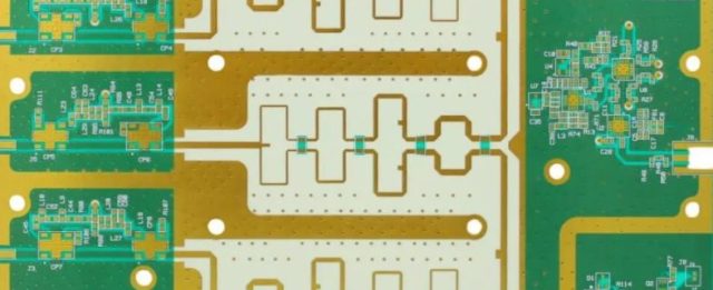
What is RF-35 PCB?

RF-35 PCB is a high-frequency laminate material developed for RF and microwave applications. It provides stable dielectric characteristics and low dissipation loss across a wide frequency range.
RF-35 material typically features:
-
Stable dielectric constant (Dk)
-
Low dissipation factor (Df)
-
Good thermal stability
-
Excellent dimensional stability
These properties make RF-35 suitable for controlled impedance circuits and high-frequency signal transmission.
Key Material Properties of RF-35 PCB
RF-35 laminates are designed to deliver reliable RF performance.
Typical characteristics include:
-
Dielectric Constant (Dk): ~3.5
-
Low Dissipation Factor (Df) for reduced signal loss
-
Low moisture absorption
-
Stable electrical performance across temperature variations
The stable dielectric properties help maintain consistent signal integrity in RF circuit designs.
Advantages of RF-35 PCB

1. Low Signal Loss
RF-35 materials are engineered to minimize dielectric loss, which is essential for maintaining signal strength in RF and microwave circuits.
Lower signal loss improves:
-
RF transmission efficiency
-
Antenna performance
-
Communication system reliability
2. Stable Dielectric Performance
A consistent dielectric constant ensures accurate impedance control, which is critical in high-frequency PCB design.
This stability supports applications such as:
-
RF filters
-
RF amplifiers
-
Antenna feed networks
3. Good Thermal Stability
RF-35 PCB materials maintain stable electrical properties across varying temperatures. This allows RF circuits to operate reliably in demanding environments.
4. Cost-Effective High-Frequency Solution
Compared with some premium RF materials, RF-35 provides a cost-efficient option for many RF applications while still delivering strong electrical performance.
This makes it attractive for high-volume wireless communication products.
Typical Applications of RF-35 PCB
Due to its low loss and stable dielectric performance, RF-35 PCBs are widely used in RF and microwave systems, including:
-
Wireless communication equipment
-
RF antennas and antenna arrays
-
Microwave circuits
-
Radar modules
-
Satellite communication devices
-
RF power amplifiers
These applications require precise impedance control and reliable signal transmission.
Design Considerations for RF-35 PCB
When designing PCBs using RF-35 material, engineers should consider several factors:
-
Controlled impedance routing
-
Proper RF grounding structures
-
Minimizing signal path length
-
Careful stack-up design
Optimizing these parameters ensures the best RF performance and minimizes signal loss.
Conclusion
As high-frequency electronic systems continue to advance, selecting the right PCB material becomes increasingly important. RF-35 PCB provides a reliable solution for RF and microwave circuit designs by offering stable dielectric properties, low signal loss, and cost-effective performance.
With proper PCB design and manufacturing expertise, RF-35 PCBs can deliver excellent performance in wireless communication systems, radar devices, and RF electronics.
