Key Manufacturing Factors That Affect Controlled Impedance PCB Accuracy
In today’s high-speed electronics market, Controlled Impedance PCB manufacturing has become a fundamental requirement for ensuring excellent signal integrity and stable electrical performance. As operating frequencies and data transmission speeds continue to rise, even minor impedance deviations in a controlled impedance PCB can result in signal reflection, timing errors, and system instability.
For this reason, achieving high controlled impedance PCB accuracy is no longer dependent on PCB design alone. It is the result of close coordination between design intent and the entire PCB manufacturing process. This article highlights the key manufacturing factors that affect controlled impedance PCB accuracy, helping engineers and buyers better understand how fabrication quality directly impacts impedance control.
1. PCB Material Selection and Dielectric Constant Stability
In controlled impedance PCB manufacturing, PCB material selection is the foundation of impedance accuracy.
- The dielectric constant (Dk) of the laminate directly determines impedance values in a controlled impedance PCB.
- Even small Dk fluctuations can lead to measurable impedance variation, especially in high-speed PCB and high-frequency PCB applications.
- Materials such as high-performance FR-4 and Rogers laminates are widely used for stable PCB impedance control.
Maintaining material consistency across production batches is essential for repeatable controlled impedance PCB accuracy.
2. Dielectric Thickness Control in Controlled Impedance PCB Stack-up
Accurate dielectric thickness is a critical parameter in controlled impedance PCB stack-up design.
- Core and prepreg thickness variations directly affect impedance values.
- During multilayer PCB manufacturing, lamination pressure, temperature, and resin flow can change final dielectric spacing.
A precisely engineered stack-up combined with strict lamination control ensures reliable controlled impedance PCB performance.
3. Trace Width Accuracy and Etching Process Control
Trace geometry is one of the most sensitive factors affecting controlled impedance PCB accuracy.
- Over-etching or under-etching during PCB fabrication alters actual trace width.
- Copper thickness, etching chemistry, and process stability all influence PCB impedance control results.
Advanced etching techniques and in-process inspections help ensure impedance-controlled traces meet design targets.
4. Copper Thickness Management and Plating Effects
In real-world controlled impedance PCB manufacturing, final copper thickness must always be considered.
- Copper plating increases trace thickness beyond base copper values.
- Uneven copper distribution across the panel can cause impedance inconsistency.
Accurate impedance modeling must reflect final copper thickness to achieve stable controlled impedance PCB results.
5. Lamination and Pressing Process Consistency
Multilayer controlled impedance PCB production relies heavily on lamination process stability.
- Press temperature and pressure directly affect dielectric thickness.
- Resin flow behavior influences spacing between signal layers and reference planes.
Consistent lamination conditions are essential for repeatable controlled impedance PCB accuracy.
6. Solder Mask Influence on PCB Impedance Control
Although often underestimated, solder mask has a measurable effect on controlled impedance PCB performance.
- Solder mask adds an additional dielectric layer over impedance-controlled traces.
- In high-speed designs, solder mask openings or design compensation may be required to maintain target impedance.
Proper solder mask control further enhances overall PCB impedance control accuracy.
7. Controlled Impedance PCB Testing and Verification
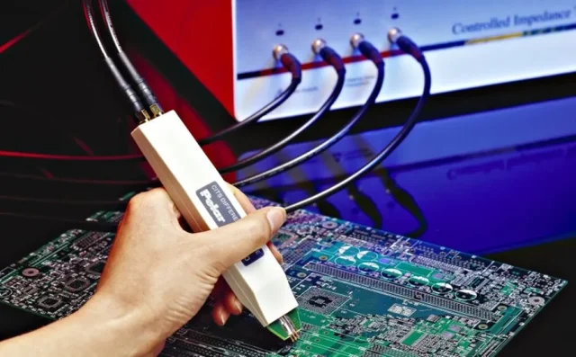
No controlled impedance PCB is complete without thorough verification.
- TDR impedance testing confirms actual impedance values after PCB manufacturing.
- Test coupons must accurately represent the production stack-up and trace geometry.
- Typical impedance tolerances include ±10%, while advanced designs may require ±5% or tighter control.
Comprehensive testing ensures every controlled impedance PCB meets customer and industry standards.
Conclusion
High controlled impedance PCB accuracy is achieved through precise control of materials, stack-up design, trace geometry, copper thickness, lamination processes, and impedance testing. Every stage of PCB manufacturing plays a critical role in final impedance performance.
By working with an experienced PCB manufacturer, engineers can achieve reliable controlled impedance PCB manufacturing, improved signal integrity, and long-term product stability.
