
In modern electronic systems, power integrity has become one of the most critical factors affecting PCB performance and reliability.
As electronic products become:
- faster,
- more compact,
- more power-dense,
- more sensitive to signal fluctuations,
power supply noise interference can create serious design challenges, including:
- unstable circuit operation,
- signal integrity degradation,
- electromagnetic interference (EMI),
- increased system errors,
- reduced product reliability.
Power supply noise is often caused by switching regulators, high-frequency digital circuits, improper grounding, poor decoupling design, and inadequate PCB layout.
A well-designed PCB must not only provide stable power delivery but also minimize noise coupling between power networks and sensitive circuits.
This article explains the main causes of power supply noise and practical PCB design methods to reduce interference.
What Is Power Supply Noise in PCB Design?
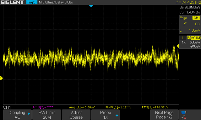
Power supply noise refers to unwanted voltage fluctuations or disturbances appearing on the power distribution network (PDN).
Ideally, a power supply should provide a clean and stable voltage. However, real circuits experience variations caused by:
- current switching,
- parasitic inductance,
- parasitic capacitance,
- voltage conversion processes,
- component operating conditions.
Common forms of power supply noise include:
Voltage Ripple
Periodic voltage variations caused by:
- switching regulators,
- DC/DC converters,
- insufficient filtering.
Transient Noise
Short-duration voltage spikes caused by:
- rapid load changes,
- digital IC switching,
- high-speed signal transitions.
Electromagnetic Coupling Noise
Noise transferred through:
- power traces,
- ground planes,
- electromagnetic radiation.
Common Causes of Power Supply Noise
1. Poor Power Distribution Network (PDN) Design
The power distribution network includes:
- power planes,
- traces,
- vias,
- capacitors,
- voltage regulators.
An inefficient PDN can introduce:
- excessive voltage drop,
- higher impedance,
- unstable power delivery.
For high-speed digital circuits, even small voltage fluctuations may affect:
- processor operation,
- memory communication,
- clock stability.
Better Approach:
Optimize the PDN by considering:
- current requirements,
- trace width,
- copper thickness,
- plane distribution,
- return current paths.
A low-impedance power network helps maintain stable voltage during dynamic load changes.
2. Insufficient Decoupling Capacitor Design
Decoupling capacitors are essential for suppressing high-frequency power noise.
When ICs switch rapidly, they require instant current supply. If the power source cannot respond quickly enough, voltage fluctuations occur.
Common Problems:
- insufficient capacitor quantity,
- incorrect capacitor placement,
- inappropriate capacitance values,
- long connection paths.
Better Approach:
Place decoupling capacitors:
- as close as possible to IC power pins,
- with short and wide connections,
- using multiple capacitor values when necessary.
Typical combinations include:
- small-value ceramic capacitors for high-frequency noise,
- larger capacitors for low-frequency fluctuations.
3. Improper Grounding Design
Grounding problems are one of the most common causes of PCB noise.
Poor ground design can create:
- ground loops,
- increased return path impedance,
- noise coupling between circuits.
Sensitive circuits such as:
- analog circuits,
- RF modules,
- ADC interfaces,
are especially vulnerable.
Better Approach:
Follow good grounding practices:
- maintain continuous ground planes,
- minimize return path length,
- separate noisy and sensitive areas,
- connect grounds properly according to system requirements.
For mixed-signal designs, careful separation between analog and digital ground regions can reduce interference.
4. Switching Regulator Noise
Switching power supplies improve efficiency but generate high-frequency noise.
Common sources include:
- MOSFET switching,
- diode recovery current,
- inductor current changes,
- high di/dt loops.
Potential Problems:
- conducted EMI,
- radiated interference,
- ripple voltage,
- interference with communication circuits.
Better Approach:
Optimize switching regulator layout:
- minimize high-current loop area,
- place input/output capacitors close to components,
- keep switching nodes away from sensitive circuits,
- use proper filtering components.
5. High-Speed Digital Circuit Switching Noise
Modern processors, FPGAs, DDR memories, and communication chips create significant switching activity.
Fast current changes can introduce:
- ground bounce,
- simultaneous switching noise (SSN),
- power rail instability.
Better Approach:
For high-speed designs:
- optimize power integrity analysis,
- improve PDN impedance,
- use appropriate layer stackup,
- maintain strong power and ground planes.
PCB Layout Techniques to Reduce Power Supply Noise
1. Optimize PCB Layer Stackup
A proper layer stackup improves:
- power integrity,
- signal integrity,
- EMI performance.
Recommended practices:
- place power and ground planes close together,
- create low-inductance current paths,
- provide continuous reference planes for high-speed signals.
For multilayer PCBs, dedicated power and ground layers can significantly reduce noise.
2. Minimize Current Loop Area
High-frequency current tends to follow the smallest impedance path.
Large current loops increase:
- electromagnetic radiation,
- noise coupling,
- EMI problems.
Design Guidelines:
- keep power paths short,
- minimize switching loops,
- place related components close together.
3. Separate Noisy and Sensitive Circuits
Different circuit blocks generate different noise levels.
High-noise areas:
- switching regulators,
- motor drivers,
- power amplifiers.
Sensitive areas:
- analog sensors,
- RF circuits,
- precision ADC circuits.
Better Approach:
Use PCB partitioning:
- isolate noisy circuits,
- control current return paths,
- avoid routing sensitive signals through noisy areas.
4. Use Ferrite Beads and EMI Filters
Ferrite beads and filters can reduce high-frequency interference between circuit sections.
They are commonly used for:
- power supply filtering,
- analog power isolation,
- RF module power filtering.
However, component selection should consider:
- frequency characteristics,
- current rating,
- impedance curve.
5. Improve Power Trace Design
Power traces carry significant current and directly affect voltage stability.
Consider:
- wider traces,
- thicker copper,
- shorter routing distance,
- multiple vias for current transfer.
For high-current applications, copper planes are usually preferred over narrow traces.
Power Integrity Testing and Validation
Proper testing helps identify hidden noise problems before mass production.
Common validation methods include:
Oscilloscope Measurement
Used to analyze:
- voltage ripple,
- transient response,
- switching noise.
Near-Field EMI Scanning
Helps locate:
- noise radiation sources,
- problematic power loops.
Power Integrity Simulation
Used during design stages to evaluate:
- PDN impedance,
- resonance points,
- voltage stability.
Advanced Techniques for Power Noise Reduction
1. PDN Optimization
Power distribution networks should be designed with:
- controlled impedance,
- low inductance,
- stable frequency response.
2. EMI Shielding
For sensitive applications, shielding methods may include:
- metal shields,
- grounding structures,
- controlled enclosure design.
3. Thermal Management Improvement
Temperature changes can influence:
- regulator efficiency,
- component characteristics,
- power stability.
Thermal design should include:
- copper areas,
- thermal vias,
- heat dissipation paths.
How KKPCB Supports Power Integrity Optimization
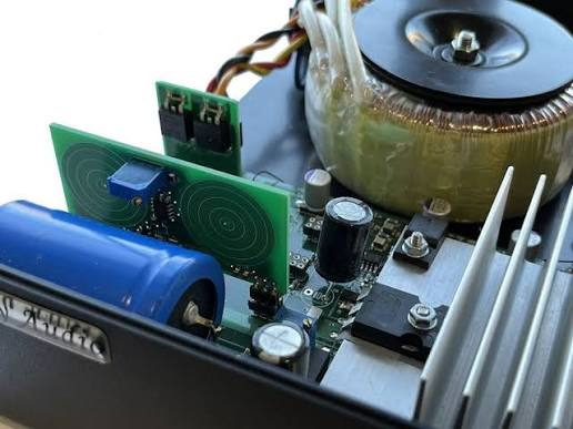
During PCB design and manufacturing, KKPCB provides engineering support including:
- PCB stackup optimization,
- power and ground plane design review,
- DFM analysis,
- impedance control,
- signal integrity evaluation,
- manufacturing feasibility assessment.
By identifying potential power integrity risks before production, engineers can improve:
- product reliability,
- manufacturing yield,
- long-term system stability.
Conclusion
Power supply noise interference is a common challenge in modern PCB design, especially for high-speed, high-density, and power-sensitive electronic products.
Effective solutions require a combination of:
- optimized PDN design,
- proper decoupling strategies,
- reliable grounding methods,
- controlled PCB layout,
- comprehensive testing.
By addressing power noise issues during the early design stage, engineers can reduce EMI risks, improve system performance, and achieve more reliable electronic products.
