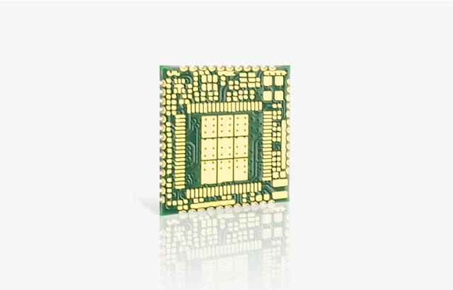
A Microvia PCB is an advanced printed circuit board technology specifically developed for HDI PCB (High Density Interconnect PCB) and high-density PCB applications. By utilizing laser-drilled microvias, Microvia PCBs enable extremely compact routing, superior signal integrity, and reliable interconnections in modern high-speed and high-frequency electronic systems.
As electronic products continue to evolve toward miniaturization, higher signal speeds, and increased functional integration, traditional through-hole PCB structures are no longer sufficient. Microvia PCB technology has become essential for meeting the design and performance requirements of 5G communication, RF modules, IoT devices, automotive electronics, and semiconductor testing systems.
Why Microvia PCB Is Essential for HDI and High-Speed PCB Applications
Compared with conventional PCB vias, a Microvia PCB dramatically increases routing density while reducing parasitic inductance and capacitance. This makes Microvia PCBs a preferred solution for high-speed PCB, controlled impedance PCB, and RF PCB designs.
Key advantages of Microvia PCB technology include:
-
Ultra-high interconnect density for fine-pitch BGA, CSP, QFN, and high pin-count ICs
-
Shorter signal paths, minimizing signal loss and reflection
-
Improved signal integrity and impedance control
-
Reduced PCB size, thickness, and overall system footprint
-
Better compatibility with HDI PCB stackups and multilayer PCB structures
By integrating Microvia PCBs, designers can achieve smaller, faster, and more reliable electronic products without increasing layer count unnecessarily.
Microvia PCB Structures and HDI Stackup Flexibility
A Microvia PCB supports multiple advanced via structures to match different performance and reliability requirements:
-
Blind Microvia PCB (outer layer to inner layer)
-
Stacked Microvia PCB for ultra-high-density HDI designs
-
Staggered Microvia PCB to enhance via reliability
-
Via-in-Pad Microvia PCB for fine-pitch and high-density component assembly
These Microvia PCB structures allow engineers to design complex multilayer PCB stackups, optimizing signal layers, power distribution, and ground referencing for high-speed and high-frequency circuits.
Microvia PCB and Controlled Impedance Performance
For high-speed PCB and RF PCB designs, maintaining precise controlled impedance is critical. Microvia PCBs significantly improve impedance performance by:
-
Eliminating long via stubs
-
Reducing signal discontinuities between layers
-
Allowing accurate reference plane transitions
-
Improving impedance consistency for differential pairs
As a result, Microvia PCBs deliver lower insertion loss, reduced jitter, and cleaner eye diagrams, especially in 5G PCB, mmWave PCB, and high-speed data transmission applications.
Applications of Microvia PCBs
Thanks to their HDI capability, high-density routing, and excellent signal integrity, Microvia PCBs are widely used in:
-
HDI PCB designs for 5G and mmWave communication modules
-
RF PCB and microwave PCB front-end circuits
-
High-speed networking and data center equipment
-
IoT PCB, wearable electronics, and compact consumer devices
-
Automotive electronics, radar systems, and ADAS modules
-
Semiconductor test PCB, ATE PCB, load board PCB, and probe card PCB
In many advanced electronic systems, Microvia PCB technology is no longer optional—it is a standard requirement.
Manufacturing Challenges and Quality Control for Microvia PCBs
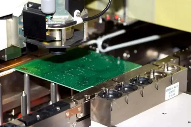
Producing a reliable Microvia PCB requires advanced manufacturing equipment and strict process control, including:
-
High-precision laser drilling for microvia formation
-
Sequential lamination for HDI PCB stackups
-
Reliable via filling and copper plating to prevent voids and cracks
-
Tight control of layer alignment and registration accuracy
-
Comprehensive AOI, X-ray inspection, microsection analysis, and electrical testing
Only an experienced Microvia PCB manufacturer can ensure long-term via reliability, especially under thermal cycling, high-speed operation, and high-frequency conditions.
Conclusion
A Microvia PCB is a cornerstone technology for HDI PCB, high-density PCB, and high-speed electronic systems. By enabling compact layouts, precise controlled impedance, and reliable multilayer interconnections, Microvia PCBs support the most demanding applications in 5G, RF, IoT, automotive, and semiconductor testing.
Selecting a professional Microvia PCB manufacturer with proven HDI and high-reliability capabilities is critical to achieving stable performance, consistent quality, and scalable production from prototype to mass manufacturing.
