A Megtron 6 PCB is a high-performance ultra low loss PCB built with Panasonic Megtron 6 laminate, designed for demanding high-speed digital and high-frequency signal applications. As next-generation electronics continue to push data rates higher—such as advanced SerDes links, high-speed networking, and data center backplanes—standard FR-4 and even some low-loss materials may struggle to meet channel loss and signal integrity requirements.
Megtron 6 PCB materials are widely used when designers require superior signal integrity, stable controlled impedance, and high reliability in complex multilayer PCB structures.
What Is Megtron 6 PCB?

A Megtron 6 PCB refers to a printed circuit board manufactured using Panasonic Megtron 6 series materials, a well-known class of high-speed laminates engineered for:
-
Ultra-low dielectric loss
-
Stable dielectric constant (Dk) performance
-
Reliable impedance control for high-speed channels
-
Strong multilayer manufacturing compatibility
Compared with standard FR-4, a Megtron 6 PCB provides significantly improved high-speed transmission performance, making it ideal for high data rate systems that require long routing lengths and tight compliance margins.
Why Choose Megtron 6 PCB for High-Speed Digital Designs?
In high-speed electronics, the PCB is part of the transmission channel. As frequencies increase, loss and distortion become major challenges. Using a Megtron 6 PCB helps reduce:
-
Insertion loss and attenuation
-
Jitter accumulation and eye closure
-
Reflection caused by impedance variation
-
Crosstalk in high-density routing environments
Megtron 6 PCB materials are commonly selected for designs that must meet strict performance requirements for modern interfaces, especially in high-layer-count and high-density PCB layouts.
Key Advantages of Megtron 6 PCB
1. Ultra-Low Loss Performance (Df) for High-Speed Channels
A Megtron 6 PCB is designed to reduce dielectric loss and improve signal transmission efficiency. Low dissipation factor (Df) helps maintain:
-
Better eye diagram performance
-
Stronger timing margin
-
Lower bit error rate (BER)
-
Longer routing capability at multi-Gbps speeds
This makes Megtron 6 PCB a preferred choice for signal integrity PCB applications where low loss is critical.
2. Stable Dielectric Constant (Dk) for Controlled Impedance PCB Design
Controlled impedance is essential for high-speed digital signals. Megtron 6 PCB materials provide stable Dk performance, supporting impedance targets such as:
-
50Ω single-ended impedance
-
90Ω / 100Ω differential impedance
Stable impedance improves channel consistency, reduces reflections, and supports reliable high-speed transmission.
3. Excellent Differential Pair PCB Routing Performance
Modern high-speed interfaces rely heavily on differential pair routing. A Megtron 6 PCB supports differential pair PCB design by enabling:
-
Consistent differential impedance control
-
Reduced skew and better matching
-
Lower loss over long routing lengths
-
Improved noise immunity and reduced EMI
This is critical for high-speed SerDes channels and data center networking links.
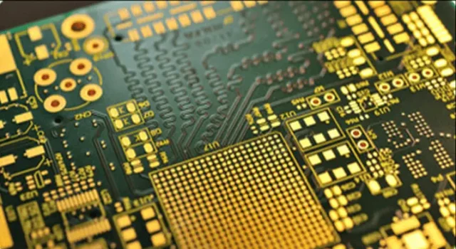
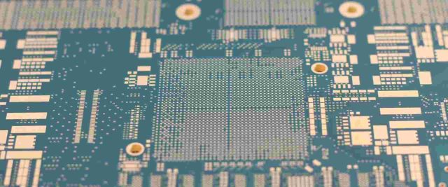
4. Strong Multilayer PCB Compatibility for Complex Stack-Ups
Megtron 6 PCB is commonly used in advanced multilayer designs, including:
-
10-layer to 20+ layer PCB stack-ups
-
High-speed backplane PCB routing structures
-
Dense BGA fanout and fine line PCB routing
-
High reliability PCB requirements for critical systems
Megtron 6 PCB materials support stable lamination performance and reliable production control.
5. Improved Signal Integrity for High-Speed Backplanes and Networking
Megtron 6 PCB materials are often used in backplanes and networking systems because they provide:
-
Lower channel loss at high frequency
-
Better performance for long trace routing
-
Stronger compliance margin for high-speed standards
-
More stable performance across different environments
For advanced networking and computing platforms, Megtron 6 PCB helps improve system reliability and data transmission stability.
Megtron 6 PCB vs Standard Megtron PCB vs FR-4
A Megtron 6 PCB is typically selected when designs require higher performance than standard low-loss laminates. Compared with FR-4, Megtron 6 PCB provides:
-
Much lower insertion loss
-
Better high-frequency stability
-
Improved signal integrity at higher data rates
-
Stronger controlled impedance consistency
Compared with general Megtron PCB materials, Megtron 6 PCB is often chosen for more demanding high-speed requirements such as long channels, backplanes, and next-gen SerDes designs.
Typical Applications of Megtron 6 PCB
Megtron 6 PCB is widely used in:
-
Data center switches, routers, and servers
-
High-speed backplane PCB systems
-
Telecom infrastructure and optical transport equipment
-
PCIe Gen4/Gen5/Gen6 high-speed boards
-
High-speed SerDes and high-speed logic PCB platforms
-
AI accelerator and GPU computing systems
-
High-speed test and validation boards
-
High reliability industrial and communication electronics
Megtron 6 PCB Design Considerations
1. Stack-Up Optimization for Low Loss PCB Routing
Megtron 6 PCB performance depends heavily on stack-up design, including:
-
Correct dielectric thickness selection for impedance targets
-
Dedicated ground reference planes for return paths
-
Proper signal layer arrangement to reduce EMI
-
Balanced structure for multilayer lamination stability
A well-optimized stack-up helps ensure controlled impedance and stable signal integrity.
2. High-Speed Differential Pair Routing Rules
For Megtron 6 PCB designs, differential pair routing should include:
-
Tight impedance control and consistent geometry
-
Accurate length matching and skew control
-
Avoiding unnecessary layer transitions
-
Proper spacing to reduce crosstalk
These practices improve overall channel performance and reliability.
3. Via Control and Backdrill Support
To reduce reflections in high-speed channels, Megtron 6 PCB designs may require:
-
Backdrilling to remove via stubs
-
Optimized via transitions for minimal discontinuity
-
Short via paths and clean reference planes
This helps maintain signal quality for multi-Gbps interconnects.
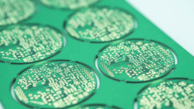
KKPCB Megtron 6 PCB Manufacturing Capabilities
KKPCB provides professional Megtron 6 PCB manufacturing services with strong engineering and quality control, including:
-
Megtron 6 PCB prototype and mass production
-
Controlled impedance PCB testing and verification
-
Multilayer Megtron 6 PCB fabrication
-
Fine line PCB routing capability for high-density designs
-
High reliability inspection, AOI, and electrical testing
-
Engineering support for stack-up planning and DFM review
We help customers achieve stable performance, consistent quality, and reliable production for Megtron 6 PCB projects.
Conclusion
A Megtron 6 PCB is an advanced ultra low loss PCB solution for high-speed digital and high-frequency electronics requiring excellent signal integrity, stable controlled impedance, and high reliability. With superior performance for long channel routing and next-gen data rates, Megtron 6 PCB is widely used in data centers, telecom infrastructure, high-speed backplanes, and advanced computing systems.
KKPCB delivers high-quality Megtron 6 PCB manufacturing with controlled impedance capability,
