What Is a Low Loss PCB?
A Low Loss PCB is a printed circuit board designed with low dielectric loss materials to minimize signal attenuation during high-frequency and high-speed signal transmission. These PCBs are critical for applications where signal integrity, phase stability, and low insertion loss are essential.
Low loss PCBs are widely used in 5G communication, RF modules, mmWave systems, automotive radar, high-speed digital electronics, and semiconductor testing equipment.
Why Low Loss PCBs Are Essential
As operating frequencies and data rates continue to increase, traditional FR-4 materials often introduce excessive signal loss and distortion. Low loss PCB technology addresses key challenges such as:
-
Signal attenuation at high frequencies
-
Dielectric loss and phase delay
-
Crosstalk and EMI issues
-
Impedance instability
-
Performance degradation over distance
Low loss PCBs enable reliable transmission of high-speed and high-frequency signals with minimal degradation.
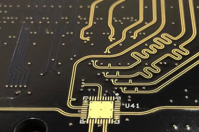
Key Features of Low Loss PCBs
A high-performance low loss PCB typically includes:
-
Low dissipation factor (Df) materials
-
Stable dielectric constant (Dk)
-
Controlled impedance traces
-
Optimized stackup design
-
Smooth copper surface treatments
These features ensure consistent electrical performance across wide frequency ranges.
Low Loss PCB Materials
Material selection is the core of low loss PCB performance. Common low loss materials include:
-
Rogers RO4003C, RO4350B
-
Rogers RT/duroid 5880, 6010
-
Megtron 6 / Megtron 7
-
Taconic RF-35, TLY series
-
Other advanced low-Df laminates
These materials provide excellent performance for RF, microwave, and high-speed digital applications.
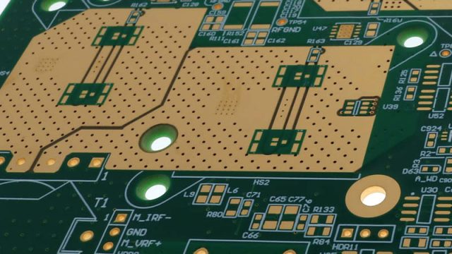
Design Considerations for Low Loss PCBs
Designing a low loss PCB requires careful attention to:
-
Stackup and dielectric thickness control
-
Trace width and spacing optimization
-
Impedance matching and length tuning
-
Via structure optimization (microvias, back drilling)
-
Minimizing signal discontinuities
Close collaboration between design and manufacturing teams helps maximize performance and yield.
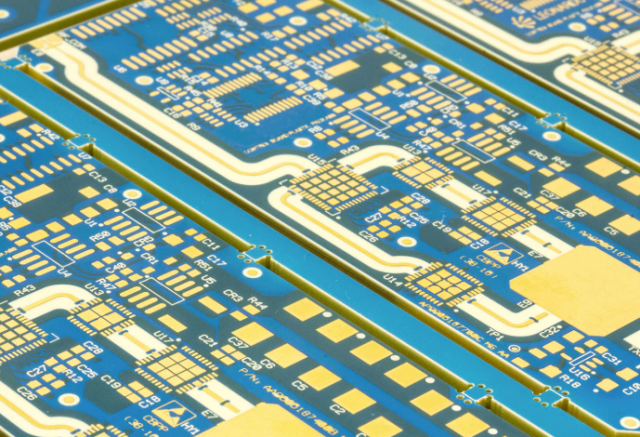
Manufacturing Capabilities for Low Loss PCBs
Low loss PCB fabrication requires advanced process control, including:
-
Precision impedance control
-
High-accuracy lamination and registration
-
Laser-drilled microvias
-
Advanced imaging and etching processes
-
Strict material handling and storage
Professional manufacturing ensures consistent quality for demanding applications.
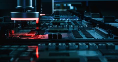
Low Loss PCB Assembly Considerations
Assembly of low loss PCBs often involves:
-
Fine-pitch and RF component placement
-
Controlled soldering profiles
-
Minimal thermal stress on special materials
-
RF connector and shielding installation
-
Electrical and RF testing
Proper assembly is essential to preserve the low loss characteristics of the PCB.
Applications of Low Loss PCBs
Low loss PCBs are commonly used in:
-
5G base stations and mmWave modules
-
RF transceivers and antenna systems
-
Automotive radar and ADAS electronics
-
High-speed networking and data centers
-
Semiconductor test boards and ATE systems
-
Aerospace and satellite communication systems
They are critical wherever signal quality cannot be compromised.
Why Choose a Professional Low Loss PCB Supplier
An experienced low loss PCB supplier provides:
-
Expertise in low-Df material processing
-
Reliable impedance-controlled manufacturing
-
Support for prototypes and small batch production
-
Consistent quality for complex RF designs
-
One-stop PCB fabrication and assembly services
The right partner helps reduce risk and accelerate product development.
