What Is an Impedance Controlled PCB?
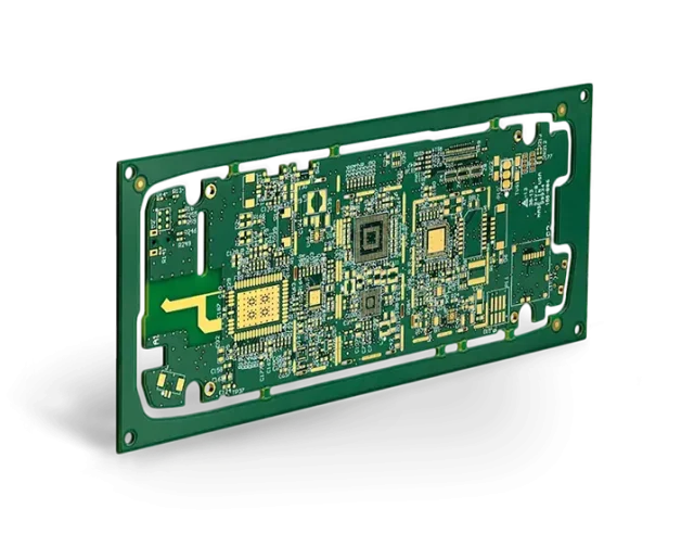
An Impedance Controlled PCB is a printed circuit board designed with precisely engineered impedance values for high-speed or high-frequency signal paths.
These PCBs ensure signal integrity, minimal reflection, and low insertion loss, which are critical for RF modules, 5G routers, high-speed digital circuits, automotive electronics, and sensor interfaces.
Key Requirements for Impedance Controlled PCB
High-quality Impedance Controlled PCBs must meet the following requirements:
-
Precise impedance tolerance (typically ±5% or better)
-
Stable dielectric constant (Dk) for consistent high-speed performance
-
Low dielectric loss (Df) for RF and high-speed signals
-
Optimized trace width, spacing, and layer stack-up
-
Reliable connector and interconnect performance
-
Thermal stability for operational environments
Meeting these requirements ensures minimal signal distortion and accurate high-speed transmission.
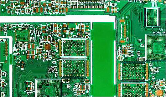
Material Selection for Impedance Controlled PCB
Material choice is critical for maintaining impedance:
-
RO4835, RO4350B, RF-35 laminates – for RF and microwave applications
-
Megtron 7 / Low-loss FR-4 hybrid laminates – for ultra-high-speed digital circuits
-
Ceramic or rigid-flex materials – for stable impedance in harsh environments
Correct material selection ensures low insertion loss and precise signal propagation.
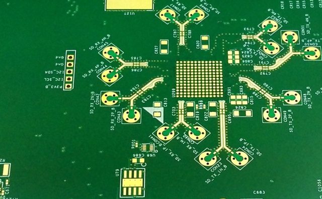
Design Considerations for Impedance Controlled PCB
Effective design strategies include:
-
Controlled microstrip and stripline trace geometry
-
Optimized power and ground plane design
-
Via fencing and shielding to reduce crosstalk
-
Proper connector and RF launch design
-
Minimized trace discontinuities and stub lengths
-
Thermal management to prevent dielectric changes
Proper design ensures high-speed data integrity and reliable RF performance.
Manufacturing Challenges of Impedance Controlled PCB
Producing a reliable Impedance Controlled PCB requires:
-
Strict dielectric and copper thickness tolerances
-
High-precision layer registration
-
Controlled copper surface roughness
-
Advanced lamination and plating processes
-
Comprehensive impedance and electrical testing
Experienced PCB manufacturers ensure consistent impedance and signal integrity.
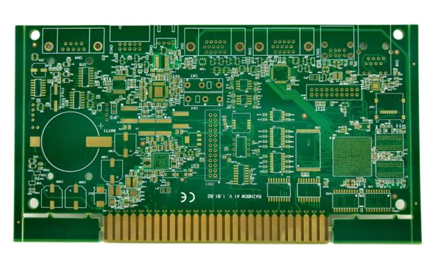
Applications of Impedance Controlled PCB
Impedance Controlled PCBs are used in:
-
5G routers and mmWave modules
-
RF Test PCBs and sensor modules
-
High-speed networking equipment
-
Automotive electronics (ADAS, radar, LiDAR)
-
Semiconductor functional test boards
-
IoT and smart device high-speed interfaces
They are essential wherever high-speed signals and RF accuracy are critical.
Conclusion
An Impedance Controlled PCB is essential for high-speed digital and RF applications that require stable signal integrity, low insertion loss, and precise impedance control.
Working with a professional Impedance Controlled PCB manufacturer ensures reliable high-frequency performance, accurate impedance, and repeatable results from prototype to volume production.
