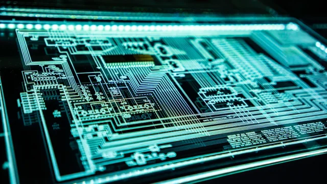
Hybrid PCB materials are engineered substrates that combine multiple material types to achieve optimized electrical, thermal, and mechanical performance in demanding electronic applications. By integrating properties of FR-4, high-frequency laminates, PTFE, or ceramic materials, hybrid PCBs enable designers to meet multi-domain requirements that a single material cannot satisfy.
Material Characteristics of Hybrid PCB Materials
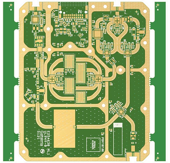
The core advantage of hybrid PCB materials is their tailored property profile, designed to balance high-speed signal integrity, thermal dissipation, and mechanical stability. Common hybrid configurations include:
-
FR-4 core with PTFE or Rogers layers for high-frequency signal routing
-
Ceramic or Aluminum Nitride sublayers for high thermal conductivity
-
Mixed laminate stackups for differential signal and controlled impedance applications
Key characteristics include:
-
Controlled dielectric constant (Dk) and low dissipation factor (Df) in high-speed layers
-
High Tg and low CTE to maintain mechanical integrity under thermal cycling
-
Enhanced thermal conductivity for heat management in power modules
-
Compatibility with multilayer stackups for complex routing and dense interconnects
Hybrid PCB materials are therefore ideal for applications requiring both high-speed RF performance and robust thermal reliability.
Electrical Performance and Signal Integrity
In modern electronic systems, hybrid PCB materials allow engineers to optimize signal paths without sacrificing thermal or mechanical stability. By isolating high-speed traces on low-loss layers while supporting the overall board with cost-effective FR-4 or high-TG layers, hybrid PCBs provide:
-
Stable impedance control for multi-layer routing
-
Reduced insertion loss and reflection in RF and microwave circuits
-
Improved phase stability in high-speed digital channels
-
Reduced crosstalk in dense multilayer routing
These advantages are crucial in 5G front-end modules, satellite communications, radar electronics, and high-speed computing boards.
Thermal and Mechanical Benefits
Hybrid PCB materials often incorporate high-TG or ceramic layers to manage localized thermal loads in power-dense systems. Benefits include:
-
Efficient heat dissipation from high-power components
-
Reduced warpage and solder joint stress
-
Dimensional stability for multi-layer stackups
-
Long-term reliability under repeated thermal cycling
This makes hybrid PCB materials a preferred choice in power electronics, EV modules, and industrial automation systems.
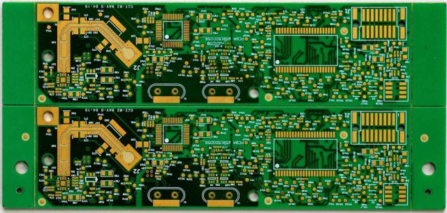
Manufacturing Considerations
Fabrication of hybrid PCB materials requires precise process control due to their multi-material nature. Key considerations include:
-
Controlled lamination pressure and temperature for heterogeneous layers
-
Fine drilling and via formation to maintain mechanical integrity
-
Etching precision for mixed material surfaces
-
Thermal and moisture management to prevent delamination or voids
Proper process control ensures that the hybrid structure delivers reliable electrical and thermal performance.
Application Domains
Hybrid PCB materials are widely used in systems that demand both electrical precision and thermal reliability, including:
-
5G and mmWave communication modules
-
Satellite and aerospace electronics
-
Power conversion and motor control boards
-
High-speed computing backplanes
-
Industrial automation and high-power driver boards
Engineering Perspective
Hybrid PCB materials provide a balanced engineering solution, combining the benefits of low-loss, high-TG, or thermally conductive materials within a single multilayer structure. By strategically selecting material combinations and controlling fabrication parameters, engineers can achieve high-performance, high-reliability PCBs suitable for advanced electronics.
KKPCB supports hybrid PCB design with material selection guidance, controlled impedance stackups, and precision multilayer fabrication, ensuring performance, thermal management, and long-term reliability.
