
With the increasing integration of digital processing, wireless communication, sensing, and power management functions, modern electronic products often combine high-speed digital circuits with sensitive analog circuits on the same PCB.
These mixed-signal systems are widely used in:
- Industrial control equipment
- Medical devices
- Automotive electronics
- Communication systems
- Data acquisition equipment
- IoT devices
However, combining high-speed digital signals and precision analog circuits creates significant PCB design challenges. Fast switching signals can generate electromagnetic noise, while sensitive analog circuits may be affected by interference from digital and power sections.
A successful mixed-signal PCB design requires careful consideration of signal integrity, power integrity, grounding, routing, and electromagnetic compatibility (EMC).
This article discusses common pitfalls in high-speed mixed-signal PCB design and practical methods to improve system reliability.
1. Understanding Mixed-Signal PCB Design Challenges
A mixed-signal PCB typically contains:
- High-speed digital circuits
- Analog signal processing circuits
- Power supply circuits
- Communication interfaces
- Sensors and measurement circuits
Each circuit type has different requirements.
Digital Circuit Characteristics
High-speed digital circuits generate:
- Rapid voltage transitions
- Harmonic noise
- Large transient currents
- Electromagnetic radiation
Examples include:
- Microprocessors
- FPGAs
- DDR memory
- High-speed communication interfaces
Analog Circuit Characteristics
Analog circuits are often sensitive to small voltage variations and external noise.
Examples include:
- ADC/DAC circuits
- Sensor interfaces
- Amplifiers
- Signal conditioning circuits
Even small interference levels may affect measurement accuracy and system performance.
2. Avoid Poor Functional Partitioning
One of the most common mistakes in mixed-signal PCB design is improper functional separation.
A PCB should be divided into different functional areas:
- Digital processing area
- Analog signal area
- Power conversion area
- RF communication area
Common Design Mistake
Placing noisy digital circuits too close to sensitive analog components may cause:
- Signal distortion
- Increased noise floor
- Reduced measurement accuracy
For example, placing a high-speed processor next to a precision ADC without proper isolation may introduce clock noise into analog measurements.
Recommended Practice
During initial PCB planning:
- Separate noisy and sensitive circuits physically
- Define clear signal flow paths
- Place critical components before routing
- Reserve dedicated areas for analog and digital sections
3. Grounding Design Pitfalls
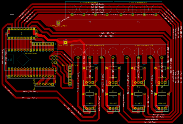
Grounding is one of the most critical aspects of mixed-signal PCB design.
Incorrect grounding methods may create:
- Ground loops
- Noise coupling
- Voltage fluctuations
- EMI problems
Avoid Random Ground Splitting
A common misconception is that separating analog ground and digital ground completely always improves performance.
However, improper ground separation may create:
- Unexpected return paths
- Increased electromagnetic radiation
- Higher impedance connections
The correct grounding strategy depends on:
- Frequency range
- Signal type
- Current flow
- PCB stack-up structure
Maintain Proper Return Current Paths
High-frequency currents follow the path of least impedance.
Design considerations:
- Provide continuous reference planes
- Avoid routing signals across ground gaps
- Keep return paths short
- Use appropriate via connections
A well-designed return path helps reduce noise and improve signal integrity.
4. High-Speed Signal Routing Mistakes
At high frequencies, PCB traces behave as transmission lines rather than simple conductors.
Incorrect routing can lead to:
- Signal reflection
- Crosstalk
- Timing errors
- Data corruption
Avoid Excessive Trace Length
Long traces increase:
- Signal attenuation
- Propagation delay
- Electromagnetic radiation
Critical high-speed signals should be routed with minimum unnecessary length.
Control Impedance
High-speed interfaces require controlled impedance routing.
Important parameters include:
- Trace width
- Dielectric thickness
- Copper thickness
- PCB material properties
Common impedance requirements:
- 50Ω single-ended signals
- 90Ω differential signals
- 100Ω differential signals
Impedance mismatch can cause reflections and reduce signal quality.
Manage Differential Pair Routing
For differential signals:
- Maintain consistent spacing
- Match trace lengths
- Avoid unnecessary layer changes
- Keep reference planes continuous
Common differential interfaces include:
- USB
- Ethernet
- PCIe
- LVDS
5. Power Integrity Problems in Mixed-Signal Systems
Power supply noise is a major source of interference in high-speed PCB designs.
Common issues include:
- Voltage ripple
- Ground bounce
- Switching noise
- Insufficient current delivery
Optimize Decoupling Capacitor Placement
Decoupling capacitors should be:
- Located close to IC power pins
- Connected with short traces
- Properly connected to ground
Poor capacitor placement reduces filtering effectiveness.
Design a Stable Power Distribution Network (PDN)
A good PDN should provide:
- Low impedance power delivery
- Stable voltage levels
- Reduced high-frequency noise
Considerations include:
- Power plane design
- Capacitor selection
- Current return paths
- Frequency response
6. EMI and EMC Design Considerations
High-speed digital circuits are common sources of electromagnetic interference.
Potential EMI sources include:
- Clock signals
- Switching regulators
- High-speed data buses
- Processor interfaces
Reduce Radiation Sources
Recommended practices:
- Minimize high-frequency current loops
- Keep clock traces short
- Avoid unnecessary trace stubs
- Use proper termination methods
Improve Circuit Isolation
Isolation methods include:
- Ground shielding
- Guard traces
- Ground via stitching
- Metal shielding structures
These methods help prevent noise coupling between circuit blocks.
7. Clock Signal Design Considerations
Clock signals often become major EMI sources because they contain high-frequency harmonics.
Common mistakes include:
- Long clock traces
- Poor impedance matching
- Routing near analog circuits
Best Practices for Clock Routing
- Keep clock traces short
- Avoid parallel routing with sensitive signals
- Use controlled impedance structures
- Provide proper termination when required
8. PCB Stack-Up Design for Mixed-Signal Systems
A properly designed PCB stack-up improves both signal integrity and EMC performance.
Important considerations include:
Dedicated Reference Planes
Continuous ground planes provide:
- Stable return paths
- Reduced radiation
- Improved signal quality
Signal Layer Arrangement
High-speed signals should be routed:
- Close to reference planes
- Away from noisy power sections
- With controlled impedance structures
Material Selection
For high-speed systems, PCB materials should provide:
- Stable dielectric constant
- Low dielectric loss
- Controlled electrical performance
High-frequency materials such as Rogers laminates may be considered for demanding applications.
9. Manufacturing Considerations for High-Speed Mixed-Signal PCBs
A high-performance design must also consider manufacturing capability.
Important factors include:
Impedance Control
Manufacturers should verify impedance through:
- TDR testing
- Stack-up control
- Material consistency
Layer Registration Accuracy
Misalignment may affect:
- Differential impedance
- Signal performance
- Via reliability
Surface Finish Selection
Surface finishes influence:
- High-frequency signal transmission
- Assembly reliability
- Long-term performance
Common options include:
- ENIG
- ENEPIG
- Immersion silver
10. Verification and Testing Before Production
Simulation and testing help identify potential issues before mass production.
Signal Integrity Analysis
Used to evaluate:
- Reflection
- Crosstalk
- Timing margins
- Eye diagrams
Power Integrity Analysis
Helps analyze:
- Voltage stability
- Current distribution
- PDN performance
EMC Testing
Includes:
- Radiated emission testing
- Conducted emission testing
- Immunity testing
Early validation reduces redesign risks.
Common Mixed-Signal PCB Design Mistakes
The following issues frequently affect product performance:
- Poor separation between analog and digital circuits
- Incorrect grounding strategy
- Insufficient power decoupling
- Ignoring controlled impedance requirements
- Routing high-speed signals across split planes
- Lack of EMC consideration during early design
- Ignoring PCB manufacturing limitations
Avoiding these mistakes can significantly improve first-pass production success.
Conclusion
High-speed mixed-signal PCB design requires balancing the requirements of digital performance, analog accuracy, power stability, and electromagnetic compatibility.
The most important design principles include:
- Proper functional partitioning
- Controlled impedance routing
- Reliable grounding strategies
- Optimized power distribution
- Effective EMI control
- Manufacturing-aware design practices
By addressing these challenges during the early PCB design stage, engineers can improve signal integrity, reduce debugging time, and achieve more reliable electronic products.
As electronic systems continue moving toward higher speeds and greater integration, advanced mixed-signal PCB design capabilities will remain essential for next-generation technologies.
