With the rapid development of modern electronics, devices are required to process and transmit data at increasingly higher speeds. Technologies such as high-performance computing, 5G networks, data centers, and advanced communication systems all rely on fast digital circuits.
At the core of these systems is the High Speed PCB, a specialized printed circuit board designed to support high-frequency digital signals while maintaining signal integrity and system reliability. High speed PCB design involves careful control of electrical characteristics such as impedance, timing, and electromagnetic interference.
What is a High Speed PCB?
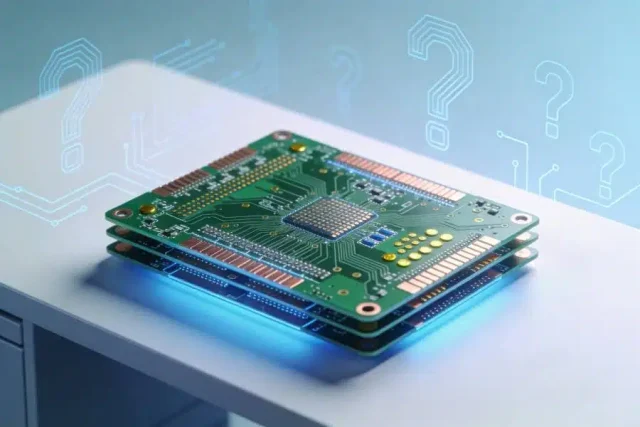
A High Speed PCB is a circuit board engineered to support digital signals operating at very high data rates, typically ranging from hundreds of megahertz to several gigahertz.
Unlike standard PCBs, high speed PCBs must address challenges such as:
-
Signal reflections
-
Crosstalk between traces
-
Transmission line effects
-
Electromagnetic interference
These challenges require advanced PCB design techniques and precise manufacturing control.
Key Design Requirements for High Speed PCB
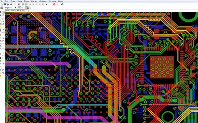
1. Controlled Impedance Routing
High speed signals behave like transmission lines. To ensure proper signal propagation, PCB traces must maintain consistent impedance.
Common impedance structures include:
-
Single-ended impedance lines
-
Differential pair routing
Accurate control of trace width, spacing, and dielectric thickness helps maintain stable impedance.
2. Signal Integrity Management
Signal integrity is one of the most critical aspects of high speed PCB design. Poor signal integrity can result in data errors and unstable system performance.
Design techniques used to improve signal integrity include:
-
Short and direct signal paths
-
Proper termination methods
-
Ground reference planes
-
Differential pair routing
These techniques help reduce reflections and signal distortion.
3. Crosstalk Reduction
When signals travel through closely spaced traces, electromagnetic coupling may occur, causing crosstalk.
To minimize this effect, designers often:
-
Increase trace spacing
-
Use ground shielding traces
-
Implement multilayer PCB stack-ups
These strategies help isolate high-speed signals.
4. Layer Stack-Up Design
A well-designed multilayer stack-up is essential for high speed PCB performance.
Typical stack-up features include:
-
Dedicated power planes
-
Continuous ground planes
-
Controlled dielectric thickness
These layers help provide stable return paths and reduce electromagnetic noise.
5. Thermal Management
High-performance electronic systems generate significant heat during operation.
Thermal design solutions may include:
-
Copper planes for heat spreading
-
Thermal vias
-
Optimized component placement
Proper heat management improves system stability and reliability.
Materials Used in High Speed PCB
High speed PCBs often require materials with stable dielectric properties and low signal loss.
Common materials include:
-
High-performance FR-4 materials
-
Low-loss laminates
-
PTFE-based substrates for extreme speeds
-
Advanced high-frequency composite materials
Selecting the appropriate material is critical for maintaining signal performance.
Applications of High Speed PCB
High speed PCBs are widely used in advanced electronic systems where fast data transmission is required.
Typical applications include:
-
Data center networking equipment
-
High-performance computing systems
-
5G communication infrastructure
-
High-speed storage devices
-
AI and cloud computing hardware
These applications require reliable high-speed signal transmission.
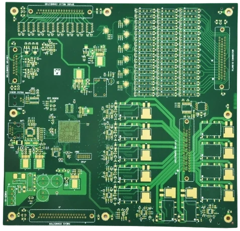
Manufacturing Considerations
Manufacturing high speed PCBs requires tight tolerances and advanced fabrication technologies.
Important manufacturing requirements include:
-
Precision impedance control
-
Fine trace width and spacing
-
Accurate multilayer lamination
-
Advanced testing and inspection
These processes ensure consistent electrical performance and manufacturing quality.
Conclusion
High speed PCB technology plays a crucial role in enabling modern digital systems that require fast and reliable data transmission. Through careful design, advanced materials, and precise manufacturing techniques, high speed PCBs ensure signal integrity and system stability in high-performance electronic devices.
As technologies such as cloud computing, artificial intelligence, and 5G networks continue to grow, high speed PCB design will remain essential for the next generation of high-performance electronics.
