System Complexity as the Driving Force
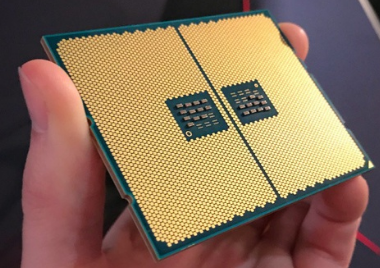
Modern electronic systems are no longer defined by individual components, but by highly integrated devices with massive I/O requirements. CPUs, GPUs, FPGAs, and advanced SoCs now feature hundreds to thousands of pins, driving the need for High Pin Count PCBs.
This shift introduces a new level of complexity:
- Multiple high-speed interfaces operating simultaneously
- Dense power and ground distribution networks
- Tight space constraints with increasing functionality
In this context, the PCB evolves from a simple interconnect into a system-level integration platform, where routing, power delivery, and signal integrity must be engineered together.
The Real Challenge: Package Breakout
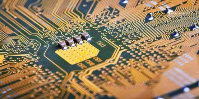
The most critical challenge in high pin count PCB design lies in breaking out signals from fine-pitch packages, especially BGAs.
- Fine Pitch Constraints:
Modern packages may have pitches of 0.8 mm, 0.5 mm, or even smaller, limiting routing channels. - Escape Routing Bottlenecks:
Efficiently routing signals away from dense pin fields requires precise planning and advanced techniques. - Layer Consumption:
Poor breakout strategy can quickly consume routing layers, increasing cost and complexity.
To address this, designers rely on:
- Microvias and HDI structures
- Via-in-pad technology
- Staggered or stacked via configurations
The breakout phase often determines whether the design is feasible, scalable, and manufacturable.
Advanced Design Techniques
To successfully manage high pin count designs, engineers apply a combination of advanced techniques:
- HDI Stack-Ups:
Using configurations like 1+N+1 or 2+N+2 to maximize routing efficiency. - Signal Layer Segmentation:
Separating high-speed, RF, and low-speed signals to minimize interference. - Length Matching & Timing Control:
Critical for high-speed buses such as DDR and SerDes. - Power Distribution Optimization:
Designing a low-impedance PDN to support dynamic current demands. - Via Optimization:
Reducing via stubs through back-drilling or blind/buried vias.
These techniques transform a High pin count PCB from a routing challenge into a controlled, high-performance system design.
Manufacturability & Cost Considerations
High pin count PCBs push fabrication capabilities and budgets simultaneously.
- Fine Line & Spacing Requirements:
Advanced processes are required to achieve tight geometries. - Multiple Lamination Cycles:
HDI designs increase process complexity and cost. - Yield Sensitivity:
Small defects can have large impacts due to design density. - Assembly Challenges:
Fine-pitch components require precise soldering and inspection. - Cost Scaling:
Costs increase with layer count, via complexity, and material selection.
Balancing performance with manufacturability is critical. Early collaboration with the PCB manufacturer helps ensure the design is optimized for both cost and yield.
Decision Guide: When Is It Worth It?
Not every design requires a high pin count PCB. The decision should be based on clear technical needs:
Use a high pin count PCB when:
- Your design includes large BGAs or advanced SoCs
- Routing congestion limits performance or scalability
- You require multiple high-speed interfaces
- Board size must be minimized without reducing functionality
Avoid unnecessary complexity when:
- Standard multilayer routing can meet requirements
- Cost sensitivity outweighs performance gains
In many cases, the goal is not simply to handle more pins—but to enable a scalable and reliable system architecture.
Final Thoughts
High pin count PCBs represent one of the most demanding areas of PCB design, where density, speed, and manufacturability must be carefully balanced.
By applying advanced breakout strategies, HDI technologies, and optimized stack-ups, engineers can transform complexity into performance.
At KKPCB, we support high pin count PCB projects with DFM collaboration, advanced fabrication capabilities, and strict quality control, ensuring designs are both high-performing and production-ready.
