Why High Pin Count Matters
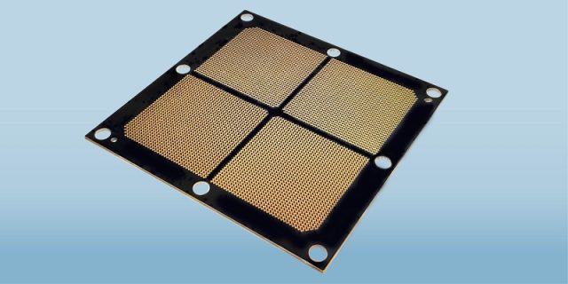
As modern electronic systems evolve, integrated circuits such as CPUs, GPUs, FPGAs, and high-speed SoCs demand hundreds or even thousands of I/O connections. A High Pin Count PCB is designed to support these devices by enabling dense interconnections within limited board space.
Unlike standard PCB designs, high pin count boards are not just about adding more pads—they require a complete redesign of routing strategy, layer stack-up, and signal management.
These PCBs are commonly found in:
- High-performance computing systems
- Networking and telecom infrastructure
- Semiconductor testing equipment (ATE, load boards)
- Advanced industrial and embedded systems
In these applications, the PCB becomes a critical platform for managing complexity, speed, and reliability.
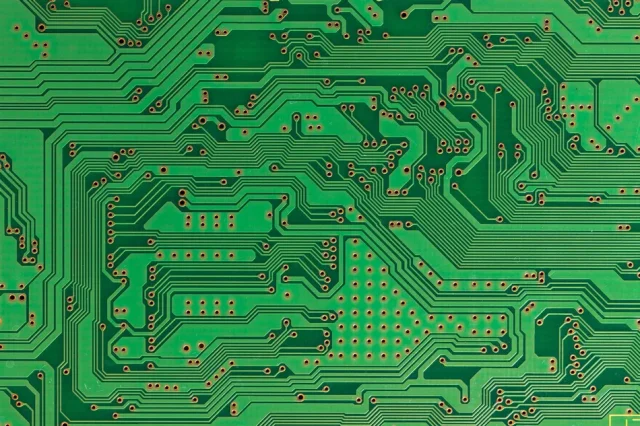
Routing Strategy for High-Density Interconnects
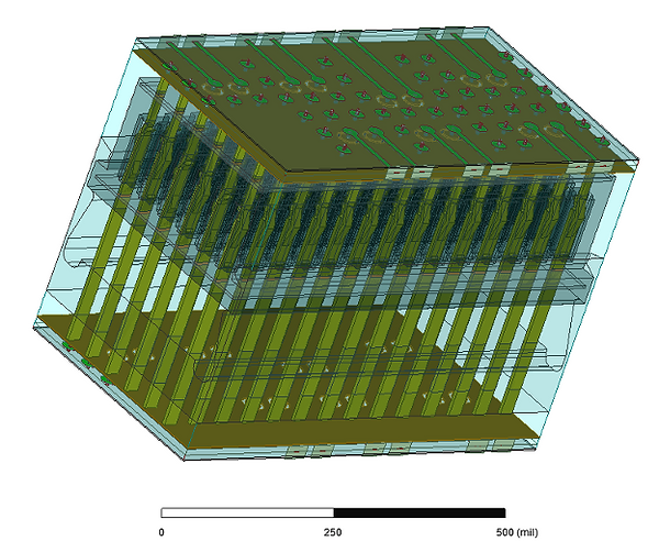
Routing is the core challenge in high pin count PCB design.
- Fan-Out Techniques:
Ball Grid Array (BGA) and fine-pitch components require advanced fan-out strategies, often using microvias and HDI structures. - Layer Expansion:
High pin count designs typically require 10–30+ layers to accommodate signal routing, power distribution, and ground shielding. - Escape Routing Optimization:
Efficient breakout routing from dense packages reduces congestion and improves manufacturability. - Via Strategy:
Blind vias, buried vias, and via-in-pad technologies are used to maximize routing space while maintaining electrical performance. - Symmetrical Stack-Up:
Ensures mechanical stability and minimizes warpage during fabrication and assembly.
A well-designed routing strategy ensures that high pin count devices can be integrated without compromising performance.
Signal & Power Integrity Challenges
With increasing pin count comes increased complexity in electrical behavior:
- Signal Integrity (SI):
High-speed signals (PCIe, DDR, SerDes) require controlled impedance, minimal reflections, and low crosstalk. - Power Integrity (PI):
Large numbers of power pins demand a low-impedance power distribution network (PDN) to prevent voltage fluctuations. - Crosstalk Management:
Dense routing increases the risk of interference between adjacent signals. - Return Path Continuity:
Maintaining solid ground references is critical for stable high-speed performance. - Thermal Density:
High pin count devices often generate significant heat, requiring efficient thermal design.
These factors make high pin count PCB design a multi-disciplinary challenge involving SI, PI, and thermal engineering.
Manufacturing Constraints
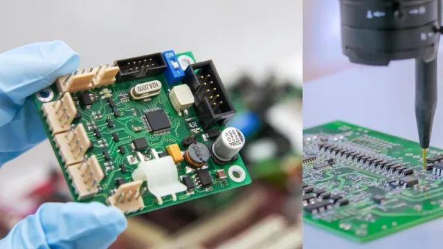
High pin count PCBs push fabrication capabilities to their limits:
- Fine Line & Spacing:
Advanced etching processes are required to achieve tight geometries. - High Layer Count Lamination:
Multiple lamination cycles must maintain precise layer alignment and structural integrity. - Via Reliability:
Microvias and via-in-pad structures must be robust to ensure long-term reliability. - Surface Finishes:
ENIG or hard gold finishes are commonly used to ensure reliable solder joints for fine-pitch components. - Quality Assurance:
- Automated optical inspection (AOI) for fine features
- X-ray inspection for BGA and via structures
- Impedance testing for high-speed traces
- Thermal and reliability testing
At KKPCB, we apply advanced manufacturing control to ensure high pin count PCBs meet both electrical and mechanical performance requirements.
When Do You Need a High Pin Count PCB?
Not every design requires this level of complexity. High pin count PCBs are essential when:
- Using large BGAs or advanced SoCs
- Designing high-speed computing or networking systems
- Developing ATE, probe cards, or load boards
- Integrating multiple high-bandwidth interfaces
- Working within space-constrained, high-density designs
If your design is limited by routing congestion or signal integrity issues, moving to a high pin count PCB architecture can provide a scalable solution.
Final Thoughts
High pin count PCBs represent the intersection of density, speed, and precision engineering. They are not simply more complex boards—they are carefully engineered systems that must balance routing efficiency, electrical performance, and manufacturability.
By combining advanced HDI techniques, optimized stack-ups, and rigorous quality control, KKPCB delivers High Pin Count PCBs that enable next-generation electronic systems to perform reliably at scale.
