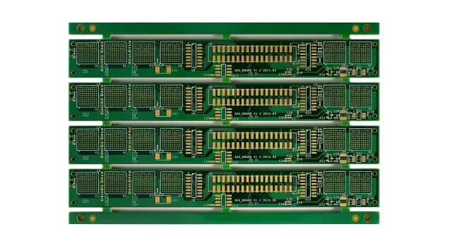
What Is a High Layer Count PCB?
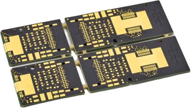
A High Layer Count PCB refers to a multilayer printed circuit board typically built with 16 layers or more, and in advanced applications, up to 40, 60, or even higher layer counts.
High Layer Count PCB is designed to support:
-
High density routing
-
Complex signal distribution
-
Controlled impedance structures
-
High speed differential pairs
-
Power and ground plane optimization
These PCBs are essential in systems where performance, miniaturization, and signal integrity are critical.
Why Use a High Layer Count PCB?
1. Support for Complex Circuit Design
As electronic systems become more powerful and compact, engineers require:
-
More routing channels
-
Multiple power domains
-
Dedicated ground planes
-
Shielding layers
High Layer Count PCB enables complex layout without increasing board size.
2. Improved Signal Integrity
High layer structures allow:
-
Proper impedance control
-
Reduced crosstalk
-
Better EMI suppression
-
Optimized return paths
This is especially important in high speed digital and high frequency applications.
3. Enhanced Power Distribution
High Layer Count PCB supports:
-
Multiple voltage rails
-
Stable power planes
-
Reduced noise coupling
-
Improved current distribution
This ensures reliable performance in high power and high speed systems.
4. Miniaturization of Advanced Systems
Instead of increasing board area, adding layers allows:
-
Compact product design
-
Dense component placement
-
Integration of advanced ICs and processors
This is essential for modern servers, telecom infrastructure, and aerospace electronics.
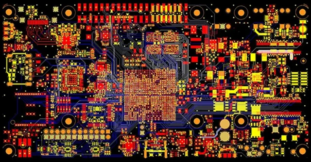
Applications of High Layer Count PCB
High Layer Count PCB is widely used in:
-
Data center servers
-
5G telecom infrastructure
-
Network switches and routers
-
Aerospace electronics
-
Military systems
-
Industrial automation controllers
-
Medical imaging equipment
These applications demand high reliability, tight impedance control, and precise layer stack-up design.
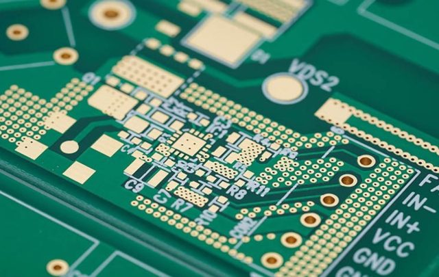
Typical Technical Capabilities
High Layer Count PCB manufacturing may include:
-
16–60+ layers
-
HDI structures with microvias
-
Blind and buried vias
-
Sequential lamination
-
Controlled impedance routing
-
Back drilling for high speed signals
-
High TG or low loss materials
Precision in layer alignment and lamination control is critical for stable production.
High Layer Count PCB vs Standard Multilayer PCB
| Feature | High Layer Count PCB | Standard Multilayer PCB |
|---|---|---|
| Layer Count | 16–60+ | 4–12 |
| Design Complexity | Very High | Moderate |
| Signal Integrity | Excellent | Standard |
| Application Level | Advanced Systems | General Electronics |
| Manufacturing Difficulty | High | Moderate |
High Layer Count PCB is engineered for high performance and mission-critical systems.
Manufacturing Challenges
Producing High Layer Count PCB requires:
-
Precise layer-to-layer alignment
-
Strict lamination pressure control
-
Low CTE material selection
-
Accurate drilling and via plating
-
Comprehensive electrical testing
Partnering with an experienced High Layer Count PCB manufacturer ensures stable yield and consistent quality.
Conclusion
High Layer Count PCB provides the structural foundation for complex, high speed, and high density electronic systems.
By enabling advanced routing, optimized signal integrity, and compact system design, High Layer Count PCB plays a critical role in modern telecom, data center, aerospace, and industrial electronics.
Choosing a reliable High Layer Count PCB supplier ensures performance, durability, and long-term system stability.
