As electronic products continue to become smaller, faster, and more complex, traditional PCB technology often reaches its physical limits. HDI PCB (High-Density Interconnect PCB) technology was developed to overcome these constraints by enabling much higher routing density, improved signal integrity, and greater design flexibility.
Today, HDI PCBs are widely used in high-speed digital systems, semiconductor testing, 5G communication, and compact electronic devices where space and performance are critical.
What Is an HDI PCB?
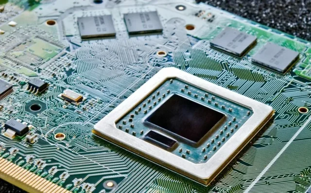
An HDI PCB is a printed circuit board that uses advanced interconnection technologies such as microvias, fine line routing, and multilayer stackups to achieve significantly higher wiring density than conventional PCBs.
Typical features of an HDI PCB include:
-
Microvias (laser-drilled vias)
-
Blind and buried vias
-
Fine line and spacing
-
Multiple lamination cycles
These features allow more connections to be placed in a smaller area without sacrificing reliability.
Why HDI PCB Technology Matters
Compared with standard multilayer PCBs, HDI PCBs offer:
-
Higher routing density for high pin count components
-
Shorter signal paths with reduced parasitics
-
Improved signal integrity for high-speed designs
-
Smaller board size and lighter weight
These advantages make HDI PCB technology essential for modern electronics.
Signal Integrity Advantages of HDI PCBs
Shorter interconnect lengths and optimized via structures give HDI PCBs clear signal integrity benefits:
-
Reduced signal delay and skew
-
Lower crosstalk between adjacent traces
-
Better impedance control for high-speed signals
As data rates increase, these characteristics become increasingly important.
Microvia Technology in HDI PCBs
Microvias are the core of HDI PCB technology. Compared to traditional through-holes, microvias offer:
-
Smaller diameter and lower parasitic capacitance
-
Improved routing flexibility
-
Better electrical performance at high frequencies
Stacked, staggered, and via-in-pad microvia structures are commonly used to support dense component layouts.
Manufacturing Challenges of HDI PCBs
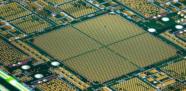
Producing reliable HDI PCBs requires advanced manufacturing capabilities:
-
Laser drilling with tight depth control
-
Precise layer alignment during lamination
-
Fine line etching accuracy
-
Strict process control to ensure via reliability
Manufacturing experience directly impacts yield and long-term performance.
Materials Used in HDI PCB Manufacturing
Material selection plays a key role in HDI PCB performance:
-
High-Tg FR-4 for cost-effective designs
-
Low-loss materials for high-speed and RF applications
-
Hybrid stackups for mixed-signal environments
Stable dielectric properties are essential for consistent electrical behavior.
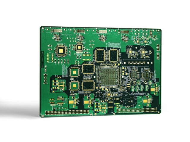
Applications of HDI PCBs
HDI PCBs are widely used in:
-
Semiconductor test and probe card systems
-
High pin count IC and BGA designs
-
5G and high-speed communication equipment
-
Automotive and industrial electronics
Their compact size and high performance support advanced system integration.
Choosing an HDI PCB Manufacturer
When selecting an HDI PCB manufacturer, key factors include:
-
Experience with microvia and multilayer HDI structures
-
Controlled impedance design and testing capability
-
Proven quality management and inspection processes
-
Ability to scale from prototype to mass production
A qualified supplier ensures consistent quality and reliable delivery.
Conclusion
HDI PCB technology enables compact, high-performance electronic designs that are not possible with traditional PCB structures. By leveraging microvias, fine line routing, and advanced manufacturing processes, HDI PCBs deliver superior signal integrity, higher routing density, and improved reliability.
Partnering with an experienced HDI PCB supplier is essential to achieving high yield and long-term performance in advanced electronic systems.
