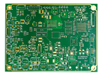
What Is a Fine Line PCB?
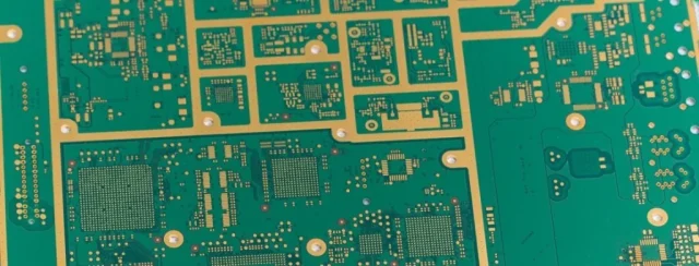
A Fine Line PCB is a printed circuit board that uses extremely narrow traces and spaces to support high-density, complex electronic designs. Fine line technology is essential for applications where board real estate is limited but high-speed performance and signal integrity are required, such as smartphones, 5G modules, high-speed computing, and semiconductor test systems.
Fine line PCBs often leverage HDI technology, microvias, and multilayer stackups to achieve dense routing.
Why Fine Line PCB Technology Matters
As electronic devices become smaller and more complex, traditional PCB trace widths cannot support modern ICs and high-speed signals. Fine line PCBs solve key challenges:
-
High pin count IC fan-out and dense component placement
-
High-speed signal routing with minimal reflection
-
Space optimization without sacrificing performance
-
Controlled impedance for high-frequency signals
-
Reliable assembly of fine-pitch components
They are critical for high-density, high-performance, and miniaturized electronics.
Key Features of Fine Line PCBs
A high-quality fine line PCB typically includes:
-
Ultra-fine trace widths and spacing (<50 μm possible)
-
HDI and microvia structures
-
Multilayer stacking for complex routing
-
Controlled impedance and signal integrity optimization
-
Optimized solder mask and surface finish
These features ensure reliable electrical performance in dense layouts.
Design Considerations for Fine Line PCBs
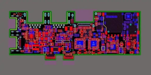
Designing a fine line PCB requires:
-
Precise trace and spacing definition
-
Proper microvia placement and fan-out strategy
-
Layer stackup optimization for high-speed and impedance control
-
Crosstalk and EMI mitigation
-
Manufacturability review to ensure assembly yield
Correct design ensures high-density routing without signal degradation.
Materials for Fine Line PCBs
Material choice is critical to maintain electrical performance:
-
High-TG FR-4 for dense digital applications
-
Low-loss laminates for RF and high-speed circuits
-
Hybrid stackups for mixed-signal integration
-
Smooth copper foils for minimal insertion loss
-
Advanced materials for automotive, 5G, and aerospace use
Proper materials preserve signal quality and reliability.
Manufacturing Capabilities for Fine Line PCBs
Producing fine line PCBs requires:
-
High-precision etching and imaging
-
Laser-drilled microvias and HDI capability
-
Tight layer-to-layer registration
-
Controlled impedance verification
-
Automated optical inspection (AOI) and electrical testing
Professional manufacturing ensures high yield and performance in micro-line layouts.
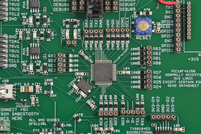
Assembly Considerations for Fine Line PCBs
Assembly includes:
-
Fine-pitch component placement and soldering
-
Reflow profile optimization for microvias and thin traces
-
X-ray inspection for hidden connections
-
Differential pair and high-speed net preservation
-
ESD-safe handling and quality verification
Correct assembly maintains signal integrity and long-term reliability.
Applications of Fine Line PCBs
Fine line PCBs are widely used in:
-
Smartphones and tablets
-
5G communication modules and mmWave systems
-
High-speed computing and networking equipment
-
Semiconductor test boards and ATE systems
-
Automotive electronics and ADAS modules
-
Aerospace and defense electronics
They are essential for compact, high-performance electronic systems.
Why Choose a Professional Fine Line PCB Manufacturer
An experienced fine line PCB manufacturer offers:
-
Expertise in HDI and fine-pitch designs
-
Advanced etching and microvia technology
-
Support for prototypes, small batches, and mass production
-
Rigorous inspection and electrical testing
-
One-stop PCB fabrication and assembly services
The right partner ensures high-density routing, signal integrity, and reliable performance.
