
Table of Contents
Duroid 6002 PCB designs can deliver a low-loss RF path, but thermal expansion, copper distribution, and connector mechanics still determine whether a microwave assembly remains stable after fabrication and reflow. The project pain point is the gap between an RF drawing and the thermal-mechanical controls used on the shop floor. This article gives a practical release framework for engineers and project managers without presenting unverified customer measurements.
Why thermal-mechanical drift matters
Every Duroid 6002 PCB is a composite structure: low-loss dielectric, copper foil, plated holes, solder mask, and hardware. Heating changes dimensions and stresses; copper planes spread heat but also affect registration and impedance. A supplier datasheet provides typical material information, while the released construction must define finished dielectric, copper, drill, and assembly assumptions.
Review the thermal path and RF path together. A high-frequency PCB design review should identify hot components, reference planes, connector datums, and keep-outs before panelization. Keep typical values, design targets, and measured results clearly separated.
Seven controls for a stable build
1. Freeze the finished stackup
Record press construction, finished dielectric targets, copper weights, bondply, and sequential-lamination steps. The stackup used for field calculations must match the construction sent to fabrication. If a proposed substitution changes thickness or copper profile, reopen the impedance and thermal review.
2. Define a continuous heat path
Show component pads, thermal vias, copper spreaders, and reference planes on one cross-section. Thermal vias should connect to the intended copper plane without creating an uncontrolled RF void. Specify the via, pad, and keep-out strategy so thermal and RF teams do not optimize different layers.
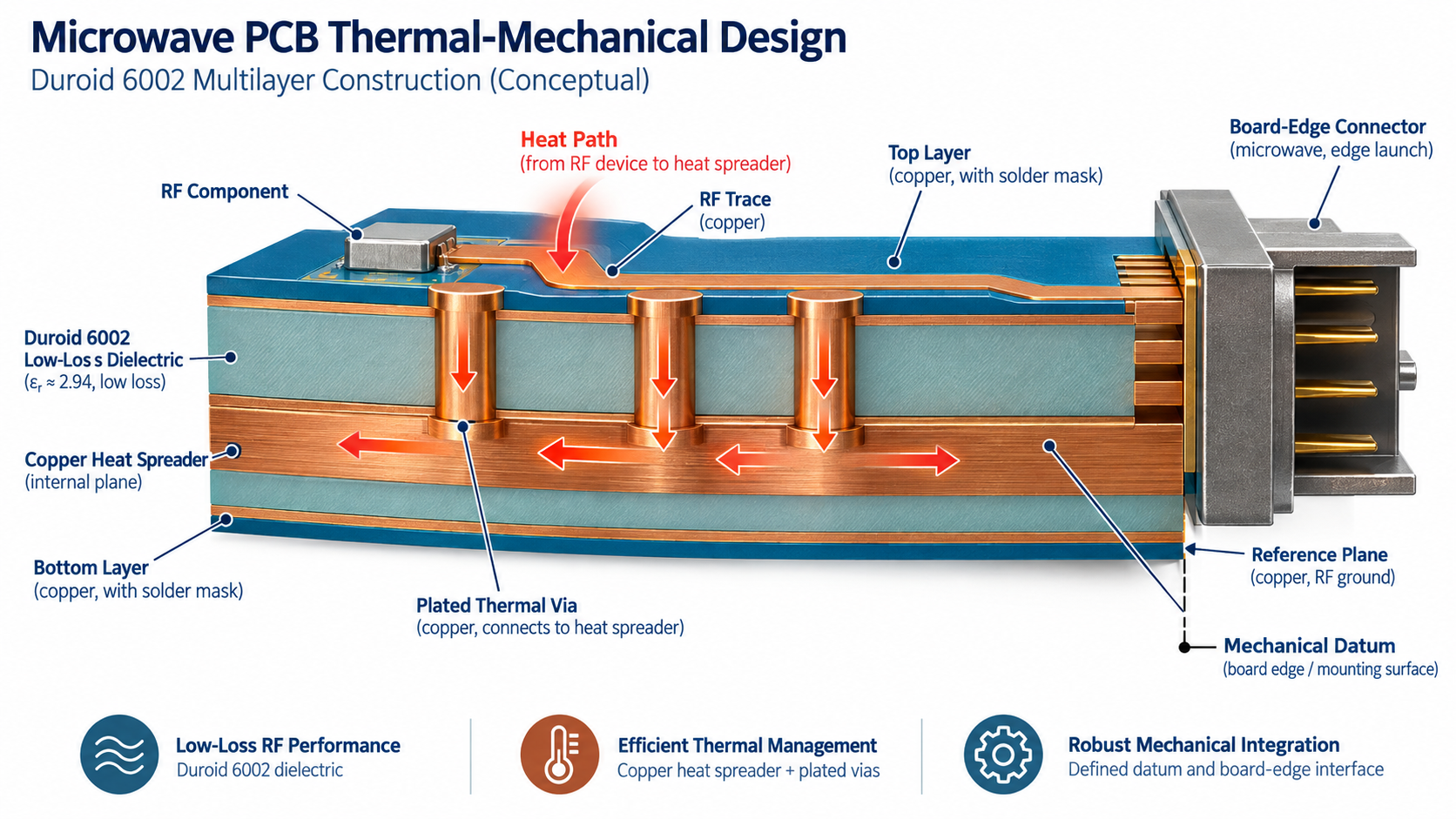
3. Balance copper and panel registration
Large copper areas can pull a panel during lamination and etch. Use a balanced panel map, tooling strategy, and fiducial plan. The PCB manufacturing traveller should tie copper balance, etch compensation, registration checks, and cross-section locations to the same revision.
4. Protect the connector launch
Connector seating, solder fillets, fixtures, and board-edge tolerances influence the electrical launch. Carry the mechanical datum from the RF drawing into the PCB assembly traveler. Mark tuning pads and mask openings as controlled features, not as guaranteed measured performance.
5. Separate conditioning from qualification
Define how material and fabricated coupons are conditioned before any environmental or RF evaluation. The sequence, dwell, and inspection method must be agreed before the build; otherwise two teams can report different results from the same lot.
6. Use representative coupons
Choose coupons that represent the critical line, via transition, or connector launch. Define coupon location, fixture, calibration, frequency range, and acceptance method. Coupon evidence is tied to the controlled revision and should not be described as a customer case study.
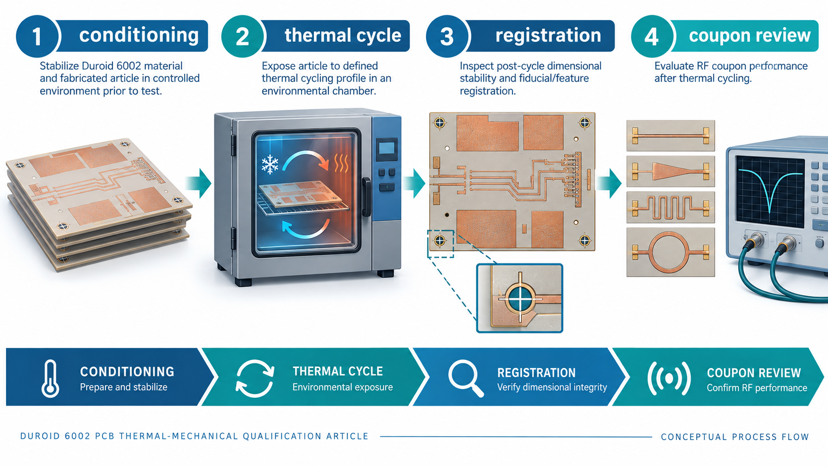
7. Carry limits into assembly and test
A multilayer PCB release should list thermal-via geometry, registration limits, connector datum, and test access. The material certificate, panel map, inspection disposition, and assembly revision should remain linked. For RF projects, the RF PCB manufacturing review should explicitly label typical, target, and measured values.
Release checklist
- Finished dielectric, copper, drill, and thermal-via targets are revision controlled.
- RF and thermal assumptions use the same cross-section and reference planes.
- Panel copper balance, fiducials, and registration checks are defined.
- Connector datums and assembly fixtures match the fabrication drawing.
- Conditioning, coupon, and acceptance methods are written before production.
- Inspection disposition is linked to the material lot and build revision.
Before release, confirm that the Duroid 6002 PCB material choice, the Duroid 6002 PCB fabrication plan, and the Duroid 6002 PCB design assumptions describe the same board. This simple alignment prevents a thermal improvement from quietly becoming an impedance or registration change.
Sources: Rogers Corporation RT/duroid 6002 material information and fabrication guidance; IPC-TM-650 methods for thermal, drilling, plating, registration, and impedance-related checks; KKPCB internal high-frequency DFM capability notes. Values are typical or target references unless explicitly identified as measured.
For a Duroid 6002 PCB thermal review, log the Duroid 6002 PCB stackup revision, Duroid 6002 PCB copper balance, Duroid 6002 PCB thermal-via map, Duroid 6002 PCB connector datum, Duroid 6002 PCB conditioning plan, and Duroid 6002 PCB coupon disposition in one release record.
