
Table of Contents
When a Duroid 6002 PCB connects a coax, edge connector, or test fixture, the launch is part of the RF circuit—not a mechanical afterthought. Engineers often see good simulated trace performance but unstable production results because the connector datum, solder-mask opening, via fence, and reference plane were never released as one structure. This guide turns that project pain point into a practical manufacturing and assembly checklist.
Why connector launches lose margin
A Duroid 6002 PCB launch combines low-loss dielectric, copper geometry, plated holes, solder, and metal hardware. Finished dielectric thickness, copper profile, pad shape, connector coplanarity, and ground-return inductance all affect the transition. Use the material supplier information as a starting point, then freeze the finished construction and drawing assumptions for the released lot.
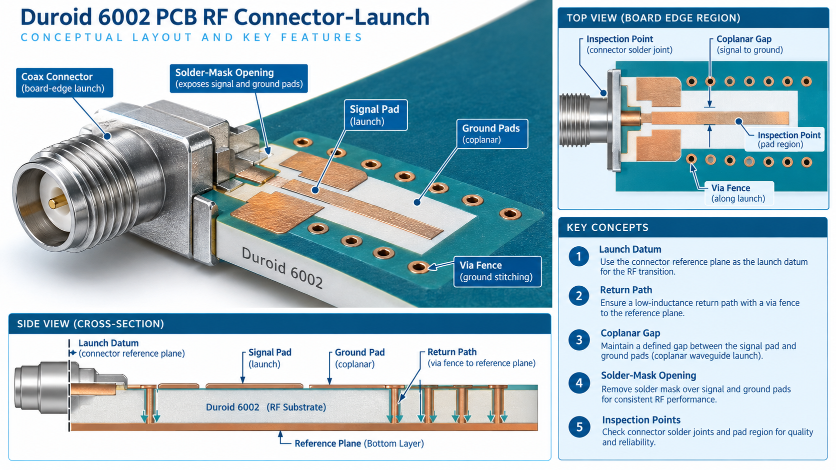
During a high-frequency PCB design review, mark the launch datum, reference plane, signal pad, ground pads, via fence, mask opening, and mechanical keep-outs. Distinguish typical material values, design targets, and measured coupon evidence.
Seven controls for reliable assembly
1. Define the launch datum
Use the connector reference plane or board edge as the datum for pad, via, and mask dimensions. Keep the datum visible in both the RF drawing and the assembly fixture. A datum that exists only in a CAD note can be lost during CAM or panelization.
2. Preserve the return path
Place ground pads and stitching vias so the return current reaches the intended reference plane with minimal discontinuity. Keep the via fence, antipad, and coplanar gap tied to the field model. Do not replace a modeled transition with a generic footprint at the last minute.
3. Control solder-mask openings
Mask clearance changes the exposed copper and can alter the local field near a launch. Specify mask opening, registration allowance, and any selective mask requirement on the fabrication drawing. The PCB manufacturing traveller should connect those dimensions to etch and plating checks.
4. Release plated-hole requirements
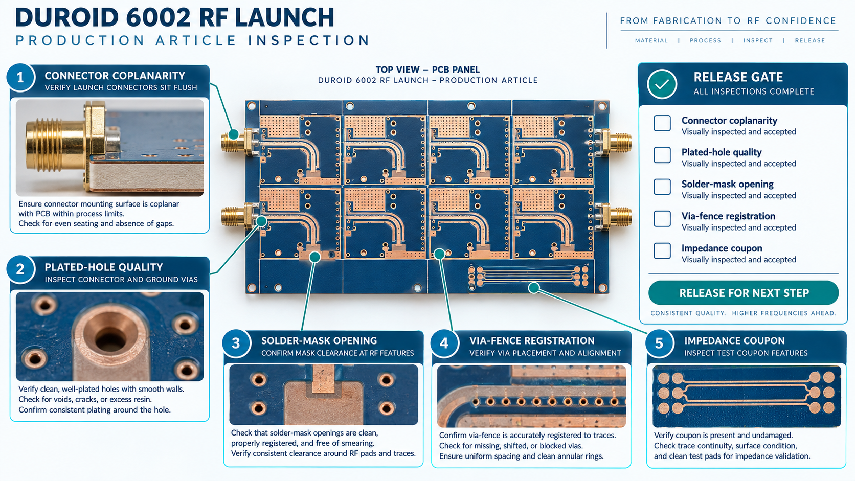
Define finished hole, annular ring, plating coverage, and allowable registration for connector and ground vias. These are manufacturing controls, not promises of a particular RF measurement. A cross-section or visual inspection plan should identify the critical holes and their disposition.
5. Keep assembly mechanics in the RF review
Connector coplanarity, solder fillets, board support, cleaning, and rework can move the launch. The PCB assembly traveler should retain the connector datum, fixture revision, and mask-opening notes. If rework is allowed, define how the RF launch is re-inspected.
6. Use a representative coupon
Choose a coupon that represents the critical line or launch, and define its fixture, calibration, frequency range, and acceptance method before panel release. Coupon evidence is tied to a controlled revision; it must not be presented as a customer case study or as a measured result unless records exist.
7. Tie panelization to the edge launch
Panel rails, tooling holes, scoring, and routing can change board-edge registration. A multilayer PCB build should identify sequential lamination, back-drill, and edge-feature constraints on the same release package. Keep the material lot, panel map, and inspection disposition linked to the revision.
Production handoff checklist
- Launch datum and connector footprint are revision controlled.
- Signal pad, ground pads, via fence, antipads, and reference plane match the RF drawing.
- Mask opening, plating, annular ring, and registration limits are manufacturable.
- Assembly fixtures and rework rules preserve connector coplanarity.
- Coupon geometry, calibration, and acceptance method are written before production.
- The RF PCB manufacturing review labels target, typical, and measured values separately.
For procurement and release alignment, the Duroid 6002 PCB material page, the Duroid 6002 PCB fabrication page, and the Duroid 6002 PCB capability page should point to the approved construction. This keeps the Duroid 6002 PCB design intent aligned with the Duroid 6002 PCB assembly handoff.
Sources: Rogers Corporation RT/duroid 6002 material information and fabrication guidance; IPC-TM-650 methods for drilling, plating, registration, assembly, and impedance-related checks; KKPCB internal high-frequency DFM capability notes. Values are typical or target references unless explicitly identified as measured.
