What Is a Differential Pair PCB?

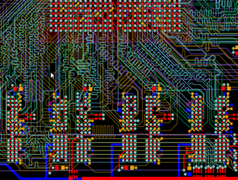
A Differential Pair PCB is a printed circuit board designed with differential signal pairs to transmit high-speed data with improved noise immunity and stable signal quality. A differential pair consists of two matched traces carrying equal and opposite signals, allowing the receiver to detect the voltage difference between them.
Differential Pair PCB routing is widely used in modern electronics because it supports high-speed, low-noise, and high-reliability signal transmission, especially for interfaces such as USB, PCIe, HDMI, DisplayPort, LVDS, Ethernet, CAN, and high-speed SerDes links.
A well-designed Differential Pair PCB improves signal integrity, reduces EMI radiation, and helps achieve consistent performance in high-speed digital systems.
Why Differential Pair PCB Routing Matters
As data rates increase and signal edges become faster, PCB traces behave like transmission lines. Without proper differential pair routing, designers may face:
-
Impedance mismatch and signal reflection
-
Increased crosstalk and noise coupling
-
Skew between the positive and negative lines
-
Reduced eye opening and higher bit error rate (BER)
-
EMI problems and compliance failures
-
Unstable high-speed communication
That’s why Differential Pair PCB design is essential for stable high-speed electronics.
Key Benefits of Differential Pair PCB Design
1. Strong Noise Immunity
Differential signaling rejects common-mode noise because both traces pick up similar interference. The receiver measures the difference, which improves stability in noisy environments.
This is a major reason Differential Pair PCBs are preferred in industrial, automotive, and high-speed networking applications.
2. Lower EMI and Better EMC Performance
A properly routed differential pair produces less radiation because the currents are equal and opposite. This helps reduce EMI and improves EMC compliance, especially for high-speed connectors and cable interfaces.
Differential Pair PCB routing is one of the most effective ways to control EMI in high-speed designs.
3. Higher Signal Integrity for High-Speed Data
Differential Pair PCBs help reduce reflection and waveform distortion when combined with:
-
Controlled impedance routing
-
Proper reference plane design
-
Stable spacing and coupling control
This results in better signal integrity and cleaner high-speed communication.
4. Stable Timing and Reduced Jitter Sensitivity
Differential pairs can provide improved timing stability compared to single-ended routing, especially in long routing paths. With good length matching and skew control, a Differential Pair PCB supports stable timing margins and reduced jitter impact.
Core Design Rules for Differential Pair PCB Routing
1. Differential Impedance Control
A Differential Pair PCB requires controlled differential impedance, commonly:
-
90Ω differential impedance (USB, many high-speed links)
-
100Ω differential impedance (Ethernet, LVDS, PCIe, HDMI, SerDes)
Maintaining consistent impedance reduces reflections and improves signal integrity.
2. Trace Spacing and Coupling
Differential pair performance depends heavily on coupling between the two traces. A Differential Pair PCB must keep:
-
Consistent spacing along the entire route
-
Smooth transitions through bends and layer changes
-
Stable coupling for predictable impedance
Improper spacing changes can cause impedance discontinuities and degrade performance.
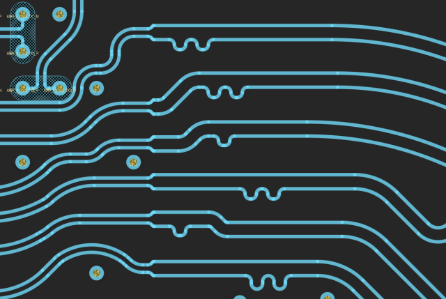
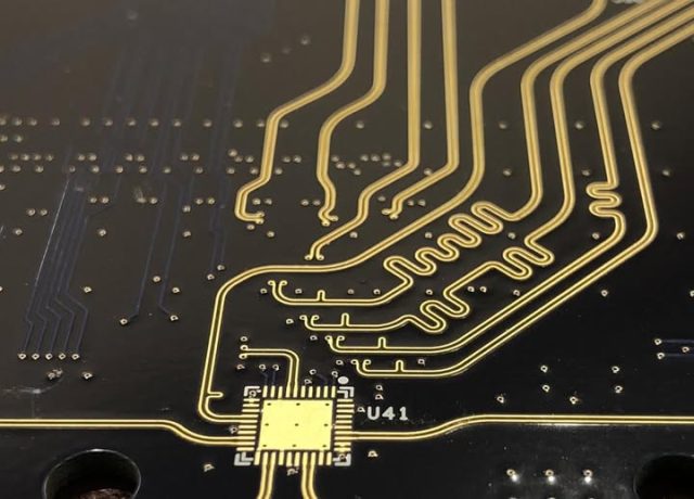
3. Length Matching and Skew Control
A Differential Pair PCB must control skew between the two traces. Best practices include:
-
Match the length of P and N traces as closely as possible
-
Use symmetric serpentine tuning if required
-
Avoid unnecessary detours that increase insertion loss
Tight length matching improves eye diagram performance and reduces timing issues.
4. Reference Plane and Return Path Continuity
Even though differential signals carry opposite currents, they still require a stable reference environment. A Differential Pair PCB should ensure:
-
Continuous ground reference planes
-
Avoiding splits or gaps under the differential pair
-
Proper plane transitions when changing layers
Good reference plane design improves signal integrity and reduces EMI.
5. Via and Layer Transition Optimization
Vias can introduce impedance discontinuities and stubs. For high-speed Differential Pair PCBs, it is important to:
-
Minimize via count on critical differential pairs
-
Use symmetrical vias for both traces
-
Maintain pair symmetry through layer transitions
-
Consider backdrill to remove via stubs (when required)
Optimized via design improves high-speed performance and reduces reflections.
6. Crosstalk Control and Routing Spacing
Differential pairs can still suffer from crosstalk if routed too close to other high-speed nets. A Differential Pair PCB should maintain:
-
Safe spacing to other signals
-
Proper layer assignment for critical pairs
-
Ground shielding or guard traces (if necessary)
This helps improve signal integrity in high-density layouts.
Typical Applications of Differential Pair PCBs
Differential Pair PCBs are essential in many advanced systems, including:
-
USB differential pair PCB (USB 2.0 / USB 3.0 / USB-C)
-
PCIe differential pair PCB (Gen3 / Gen4 / Gen5)
-
HDMI and DisplayPort differential routing
-
Ethernet differential pair PCB (1G / 10G / 25G and higher)
-
LVDS display and camera modules
-
SerDes and high-speed backplane systems
-
Automotive communication PCBs (CAN, LVDS, high-speed links)
-
IC test PCB and ATE boards requiring stable high-speed transmission
KKPCB Differential Pair PCB Manufacturing Support
KKPCB provides professional Differential Pair PCB manufacturing and engineering support to help customers achieve stable high-speed performance. Our capabilities include:
-
Controlled impedance PCB fabrication with tight tolerance
-
Multilayer PCB stack-up optimization for differential routing
-
Fine line PCB and HDI PCB manufacturing for dense routing
-
Backdrill options for via stub control
-
High reliability PCB processes and strict inspection
-
Prototype to mass production for high-speed differential pair PCBs
We help customers build Differential Pair PCBs with improved signal integrity, reduced EMI, and stable high-speed data performance.
Conclusion
A Differential Pair PCB is essential for modern high-speed digital communication, offering strong noise immunity, lower EMI, and better signal integrity. By controlling differential impedance, maintaining consistent spacing, ensuring length matching, and optimizing via transitions, Differential Pair PCBs enable reliable performance for interfaces such as USB, PCIe, HDMI, Ethernet, and SerDes.
KKPCB delivers high-quality Differential Pair PCB solutions with controlled impedance manufacturing and high reliability processes for advanced electronics.
