
With the rapid development of wireless communication, radar systems, high-speed data transmission, and advanced electronic equipment, traditional PCB technologies are facing increasing challenges in signal transmission performance.
As electronic systems continue moving toward higher frequencies and faster data rates, high-frequency PCB circuit boards have become a critical technology for ensuring stable signal transmission and reliable system performance.
Unlike conventional PCB materials, high-frequency PCBs are designed specifically for applications where electrical characteristics at high frequencies become a major consideration.
They are widely used in:
- RF communication systems
- Microwave equipment
- Automotive radar
- Satellite communication
- High-speed networking
- Industrial sensing systems
High-frequency PCB design requires comprehensive control of:
- Material properties
- Signal transmission characteristics
- Impedance performance
- Manufacturing precision
1. What Is a High-Frequency PCB?
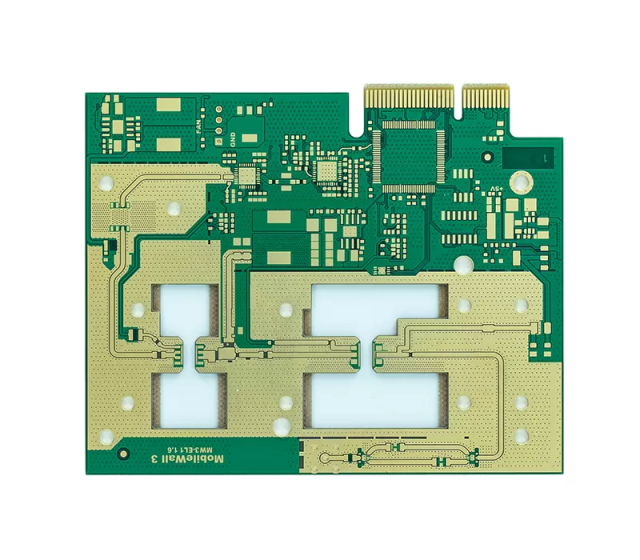
A high-frequency PCB is a printed circuit board designed to transmit electrical signals at high frequencies, typically above several hundred MHz and extending into the GHz range.
Unlike standard PCB applications that mainly focus on basic electrical connections, high-frequency PCB design treats copper traces as controlled transmission structures.
The performance of a high-frequency PCB depends heavily on:
- Dielectric constant (Dk)
- Dissipation factor (Df)
- Signal loss characteristics
- Thermal stability
- Manufacturing tolerance
High-frequency PCBs usually use specialized substrate materials instead of standard FR-4 to achieve stable electrical performance.
Common high-frequency materials include:
2. Why Are High-Frequency PCBs Important?
As electronic products become faster and more integrated, signal transmission faces several challenges.2.1 Increased Signal Loss at High Frequencies
At higher frequencies, signals are more sensitive to:
- Dielectric loss
- Copper surface roughness
- Impedance variation
These factors can reduce signal quality and system performance.
2.2 More Strict Signal Integrity Requirements
High-frequency systems require accurate control of:
- Signal amplitude
- Phase stability
- Transmission delay
Poor PCB design may result in:
- Signal attenuation
- Reflection
- Crosstalk
- Data errors
2.3 Greater Demand for Compact Integration
Modern electronic devices require:
- Smaller size
- Higher functionality
- More integrated modules
High-frequency PCBs enable compact RF and microwave circuit designs while maintaining performance.
3. Key Characteristics of High-Frequency PCB Materials
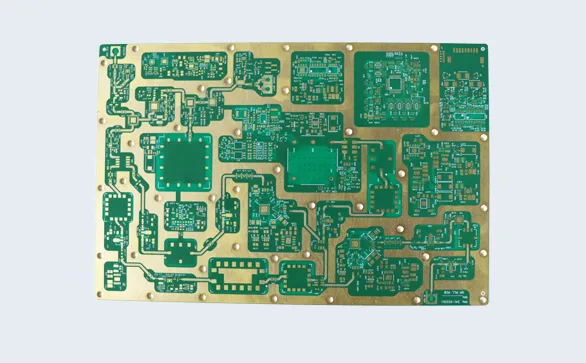
Material selection is one of the most important factors in high-frequency PCB development.
3.1 Stable Dielectric Constant (Dk)
The dielectric constant affects:
- Signal propagation speed
- Characteristic impedance
- Phase accuracy
A stable Dk value helps maintain predictable electrical performance.
This is especially important for:
- Microwave circuits
- Antenna systems
- High-speed communication equipment
3.2 Low Dissipation Factor (Df)
The dissipation factor represents dielectric energy loss.
A lower Df provides:
- Lower insertion loss
- Better transmission efficiency
- Improved signal quality
Applications requiring low-loss performance often use advanced RF materials.
3.3 Low Moisture Absorption
Moisture can influence dielectric properties and cause performance variation.
High-frequency materials typically require:
- Low moisture absorption
- Environmental stability
- Reliable long-term operation
3.4 Thermal Stability
High-frequency PCB materials should maintain stable electrical properties under temperature changes.
Important factors include:
- Thermal expansion coefficient
- Temperature coefficient of dielectric constant
- Mechanical stability
4. Types of High-Frequency PCB Materials
4.1 PTFE-Based High-Frequency PCB
PTFE materials are widely used in demanding RF and microwave applications.
Advantages:
- Extremely low dielectric loss
- Excellent high-frequency performance
- Stable electrical characteristics
Applications:
- Microwave circuits
- Radar systems
- Satellite communication
4.2 Rogers High-Frequency PCB Materials
Rogers materials are commonly used for RF and microwave PCB applications.
Typical characteristics:
- Low loss
- Stable dielectric performance
- Good thermal reliability
Common materials include:
- RO3003
- RO4003C
- RO4350B
- RO4835
4.3 Ceramic-Based High-Frequency PCB
Ceramic materials provide:
- Excellent thermal conductivity
- Stable dielectric properties
- High reliability
Applications:
- High-power RF modules
- Semiconductor applications
5. Application Scope of High-Frequency PCB
5.1 RF Communication Equipment
High-frequency PCBs are widely used in wireless communication systems.
Applications include:
- RF modules
- Base station equipment
- Wireless transceivers
Requirements:
- Low signal loss
- Stable impedance
- High-frequency reliability
5.2 Microwave Systems
Microwave circuits operate at very high frequencies and require precise electrical control.
Applications include:
- Microwave amplifiers
- Filters
- Oscillators
- Signal processing modules
High-frequency PCB materials help maintain:
- Phase consistency
- Transmission efficiency
- Signal stability
5.3 Automotive Radar Systems
Modern vehicles increasingly rely on radar sensing technologies.
77GHz radar systems require high-performance PCB solutions.
Applications include:
- Adaptive cruise control
- Blind spot detection
- Autonomous driving systems
High-frequency PCB advantages include:
- Accurate signal transmission
- Stable antenna performance
- Environmental reliability
5.4 Satellite and Aerospace Electronics
Aerospace systems require highly reliable communication and sensing equipment.
High-frequency PCBs support:
- Satellite communication
- Navigation systems
- Radar equipment
Key requirements:
- Low loss
- Thermal stability
- Long-term reliability
5.5 Industrial Sensors and IoT Devices
Industrial IoT applications increasingly require wireless connectivity.
High-frequency PCBs are used in:
- Wireless sensors
- Smart monitoring systems
- Industrial communication modules
Advantages:
- Compact design
- Stable signal performance
- Reliable operation
5.6 Semiconductor Testing Equipment
ATE (Automatic Test Equipment) and semiconductor testing systems require precise high-speed signal transmission.
High-frequency PCBs help improve:
- Test accuracy
- Signal consistency
- Measurement reliability
6. High-Frequency PCB Design Considerations
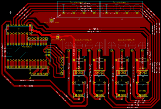
6.1 Controlled Impedance Design
Impedance control is essential for high-frequency circuits.
Factors affecting impedance include:
- Trace width
- Copper thickness
- Dielectric thickness
- Material properties
Common impedance structures include:
- Microstrip
- Stripline
- Differential pair
6.2 RF Trace Routing
High-frequency signal paths should be carefully optimized.
Design considerations include:
- Short transmission paths
- Smooth routing transitions
- Reduced unnecessary vias
Avoid:
- Sharp corners
- Sudden width changes
- Poor grounding structures
6.3 Grounding and Shielding
Proper grounding improves:
- Signal integrity
- EMI performance
- RF isolation
Common methods include:
- Continuous ground planes
- Via stitching
- Shielding structures
6.4 Stack-Up Optimization
A proper PCB stack-up helps achieve:
- Stable impedance
- Controlled signal return paths
- Reduced interference
Engineers should consider:
- Signal layer arrangement
- Reference planes
- Material combinations
7. Manufacturing Challenges of High-Frequency PCB
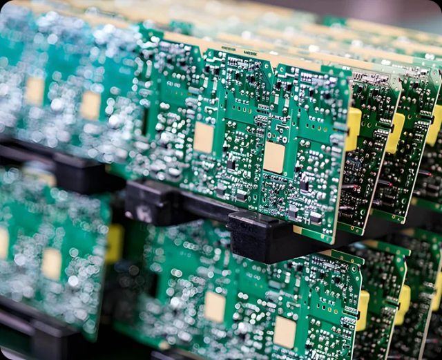
7.1 Material Processing Control
High-frequency materials may require specialized manufacturing processes.
Challenges include:
- Material handling
- Lamination control
- Dimensional stability
7.2 Impedance Accuracy
Manufacturing variations may affect:
- Trace width
- Dielectric thickness
- Final impedance value
Professional PCB manufacturers typically use:
- TDR impedance testing
- Process monitoring
- Stack-up verification
7.3 Copper Surface Roughness Control
At high frequencies, current tends to flow near the conductor surface.
Excessive copper roughness can increase:
- Insertion loss
- Signal attenuation
Low-profile copper technology may be required for advanced designs.
8. Future Development Trends of High-Frequency PCB
With the growth of:
- 5G communication
- Autonomous driving
- Artificial intelligence hardware
- Industrial automation
- Satellite systems
high-frequency PCB technology will continue evolving.
Future trends include:
- Lower-loss materials
- Higher-frequency operation
- Advanced antenna integration
- Improved thermal management
- More compact RF modules
Conclusion
High-frequency PCB circuit boards are essential components in modern electronic systems requiring reliable signal transmission at high frequencies.
Their performance depends on multiple factors, including:
From communication equipment and automotive radar to microwave systems and industrial sensors, high-frequency PCBs provide the foundation for advanced electronic technologies.
By combining suitable materials, optimized design methods, and strict manufacturing control, engineers can achieve high-performance PCB solutions capable of meeting the challenges of next-generation electronic systems.
