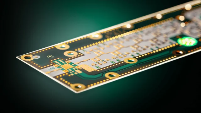
As 5G wireless infrastructure and satellite communication systems continue to evolve toward higher frequencies, wider bandwidths, and denser integration, the demand to buy high frequency PCBs with precise electrical control has increased significantly. In these applications, controlled impedance PCB design and ultra-low insertion loss PCB performance are no longer optional—they are fundamental to achieving stable signal transmission, low phase error, and predictable RF behavior across the entire operating band.
For RF engineers and system integrators working on 5G base stations, mmWave antenna arrays, satellite transceivers, and RF front-end modules, selecting the right high frequency PCB supplier is a critical engineering decision rather than a simple purchasing task.
Why Controlled Impedance Is Critical in High Frequency PCBs
Controlled impedance PCBs are essential in high-speed RF and microwave designs because signal integrity at high frequency is extremely sensitive to geometry, dielectric properties, and copper characteristics. In 5G and satellite systems, impedance mismatches can directly cause:
-
Signal reflections and return loss degradation
-
Eye diagram closure in high-speed digital interfaces
-
Phase distortion in phased-array and beamforming systems
-
Increased EMI and cross-talk between RF channels
When engineers buy high frequency PCBs, impedance control must be guaranteed not only at the design stage but also throughout fabrication. This requires tight control over trace width, dielectric thickness, copper roughness, and lamination consistency.
At KKPCB, controlled impedance PCB manufacturing is supported by stackup simulation, impedance modeling, and in-process verification to ensure each high frequency PCB meets strict tolerance requirements for RF and microwave applications.
Low Insertion Loss: A Core Requirement for 5G and Satellite PCBs
Insertion loss becomes a dominant limiting factor as operating frequencies move into the sub-6 GHz, mmWave, Ku-band, and Ka-band ranges. Excessive dielectric loss or conductor loss can significantly reduce system efficiency, especially in satellite systems where power budgets are extremely constrained.
To minimize insertion loss in high frequency PCBs, several key engineering factors must be addressed:
-
Selection of low Dk and low Df PCB materials such as Rogers, PTFE, and hybrid laminates
-
Optimization of trace geometry to reduce skin effect and conductor loss
-
Controlled copper surface roughness to balance adhesion and RF performance
-
Proper via transition design, including back-drilling or blind via structures
Buying high frequency PCBs optimized for low insertion loss ensures higher antenna gain, improved link budget, and more stable RF performance across temperature and frequency variations.
Material Selection for High Frequency and Satellite PCB Applications
Material choice is a defining factor when purchasing high frequency PCBs for 5G and satellite systems. Common material options include:
-
Rogers high frequency laminates for stable dielectric performance
-
PTFE-based materials for ultra-low dissipation factor and phase stability
-
Hybrid PCB stackups combining RF laminates with FR-4 for cost optimization
Each material system affects impedance accuracy, insertion loss, and thermal reliability differently. A qualified high frequency PCB manufacturer should provide material recommendations based on frequency range, power level, and reliability requirements rather than offering a one-size-fits-all solution.
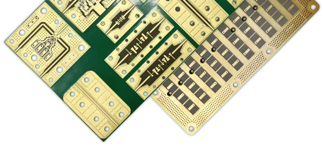
Manufacturing Precision in High Frequency PCB Fabrication
Even the best PCB design can fail if manufacturing precision is insufficient. For controlled impedance and low loss performance, high frequency PCB fabrication must include:
-
Tight lamination thickness tolerance
-
Precise impedance-controlled etching
-
Advanced registration for multilayer RF stackups
-
Consistent via drilling and plating quality
When engineers buy high frequency PCBs for 5G and satellite applications, they must evaluate the manufacturer’s ability to control these variables at scale. Process capability is as important as material selection.
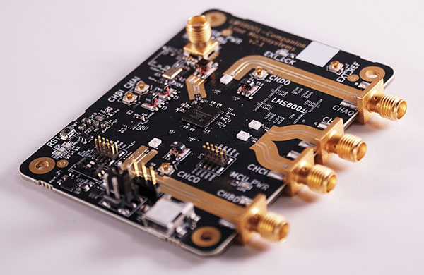
Applications in 5G and Satellite Systems
High frequency PCBs optimized for controlled impedance and low insertion loss are widely used in:
-
5G base station RF units and mmWave antenna modules
-
Satellite communication payloads and transceiver boards
-
Phased-array radar and beamforming systems
-
High-speed RF front-end and microwave modules
In all these systems, PCB performance directly impacts system-level reliability, efficiency, and signal fidelity.
Why Choose KKPCB for High Frequency PCB Manufacturing
KKPCB specializes in high frequency PCB manufacturing for demanding RF, microwave, and satellite applications. Our capabilities include controlled impedance PCB fabrication, low insertion loss PCB optimization, advanced RF material processing, and strict quality control tailored to high-frequency environments.
By working closely with engineering teams, KKPCB helps customers buy high frequency PCBs that meet real-world electrical, thermal, and reliability requirements—not just nominal design specifications.
