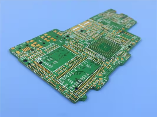
As electronic devices become smaller, faster, and more complex, PCB designers must adopt advanced interconnection technologies to achieve higher circuit density. Blind Via PCB technology is widely used in modern HDI PCB designs to enable efficient routing between layers without occupying unnecessary space on the entire board.
A Blind Via PCB uses vias that connect an outer layer to one or more inner layers, but do not pass completely through the board. This design allows engineers to increase routing density and improve overall PCB performance in compact electronic products.
What Is a Blind Via PCB?
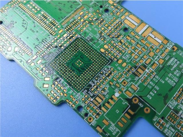
A Blind Via PCB is a printed circuit board that incorporates blind vias, which are plated holes connecting the outer layer to one or more inner layers without penetrating the entire PCB stackup.
Unlike through-hole vias, blind vias only extend partially through the board, which helps free up routing space on other layers.
Key characteristics of Blind Via PCBs include:
-
Partial-depth vias connecting surface and internal layers
-
Higher routing density in multilayer PCB designs
-
Reduced PCB size and improved layout flexibility
-
Enhanced signal performance in high-speed circuits
Blind vias are commonly used in HDI PCBs, high-speed digital circuits, and compact electronic devices.
Advantages of Blind Via PCB
1. Increased Routing Density
A Blind Via PCB allows designers to use more routing space because the vias do not pass through the entire board. This enables higher component density and more compact PCB layouts.
2. Improved Signal Integrity
By reducing unnecessary via stubs, blind vias help improve signal quality in high-speed PCB designs.
3. Smaller PCB Size
Blind via technology enables designers to create smaller and thinner multilayer PCBs, which is critical for modern compact electronics.
4. Better High-Speed Performance
Blind vias reduce signal reflections and parasitic effects, which improves performance in high-speed digital and RF circuits.
5. Enhanced HDI PCB Design
Blind vias are an essential technology for High-Density Interconnect (HDI) PCBs, allowing more complex routing within limited PCB space.
Blind Via PCB vs Through-Hole PCB
Compared with traditional through-hole vias, blind vias offer several important advantages:
-
Reduced layer-to-layer interference
-
More available routing space
-
Improved signal integrity
-
Better support for high-density PCB layouts
However, blind vias also require more advanced manufacturing processes and precise drilling technology.
Design Considerations for Blind Via PCB
When designing a Blind Via PCB, engineers must consider several key factors:
-
Proper PCB stackup planning
-
Accurate blind via depth control
-
Compatibility with HDI PCB fabrication processes
-
Controlled impedance routing for high-speed signals
-
Thermal and mechanical reliability of vias
Close collaboration with an experienced PCB manufacturer helps ensure reliable blind via implementation.
Applications of Blind Via PCB
Blind via technology is widely used in advanced electronics requiring compact and high-performance PCB designs, including:
-
Smartphones and mobile devices
-
High-speed computing hardware
-
Networking and telecom equipment
-
Aerospace electronics
-
Automotive control systems
-
Industrial automation systems
These applications rely on blind via PCBs to achieve compact layouts and reliable signal performance.
Manufacturing Requirements
Manufacturing Blind Via PCBs requires specialized PCB fabrication techniques, including:
-
Laser drilling or controlled depth mechanical drilling
-
Precision via plating processes
-
Multilayer PCB lamination technology
-
Advanced inspection and reliability testing
These processes ensure that blind vias maintain strong electrical connections and long-term reliability.
Conclusion
Blind Via PCB technology is an important solution for modern high-density multilayer PCB designs. By enabling partial-layer interconnections, blind vias improve routing density, reduce board size, and enhance signal integrity in advanced electronic systems. As electronic devices continue to shrink while increasing in complexity, Blind Via PCBs will remain a key technology in next-generation PCB design.
