Blind and Buried Vias in PCB Design — Structure, Function, and Manufacturing Insights
As the miniaturization of electronic components continues to accelerate, PCB designs must accommodate finer pitch components and higher circuit densities, especially in advanced mobile, communication, and computing applications. One of the critical technologies enabling this evolution is the use of blind and buried vias, which allow multilayer interconnection without compromising board space or signal integrity.
1. Definition and Classification
A via is a plated hole in a PCB that provides an electrical connection between different conductive layers. Based on its depth and position, vias are categorized as:
-
Through-Hole Vias: Extend through the entire board thickness.
-
Blind Vias: Connect an outer layer to one or more inner layers but do not pass through the entire PCB.
-
Buried Vias: Connect only internal layers, invisible from the board surface.
Blind vias are further divided by their manufacturing methods:
-
Photo-defined blind vias – formed using photosensitive resin and photolithography.
-
Sequential lamination blind vias – produced by multiple lamination cycles.
-
Controlled-depth drilled blind vias – mechanically drilled with precise depth control.
-
Laser-drilled blind vias – created using CO₂ or excimer lasers for high accuracy and density.
2. Technical Advantages
Blind and buried vias significantly improve signal integrity and electrical performance in high-speed designs by minimizing parasitic capacitance and inductance associated with long through-hole vias. Their reduced length and optimized aspect ratio (<1:1) enable clean, low-loss transmission for high-frequency signals (>4.8 Gb/s).
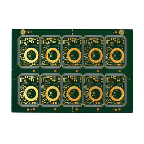
In addition, by removing unnecessary via stubs and optimizing routing density, they allow for compact BGA fan-out, supporting components with 0.5 mm or smaller pitch. This is essential in smartphone PCBs, RF modules, and high-density interconnect (HDI) systems.
3. Manufacturing Considerations
Producing blind and buried vias requires precise depth control, advanced drilling technology, and uniform plating. Improper via formation can lead to plating voids, barrel deformation, or micro-cracking—often caused by non-uniform glass weave structures in the laminate.
To ensure plating reliability, manufacturers typically limit the depth-to-diameter aspect ratio to 1:1 or less. For finer structures, copper-filled or “button-plated” vias are preferred to avoid trapped air during solder reflow, especially under BGA pads. Offset drilling can also mitigate void-induced reliability issues.
Sequential lamination and build-up processes enable stacked vias, providing vertical interconnections through multiple layers while maintaining mechanical integrity and electrical performance.
4. Applications and Design Implications
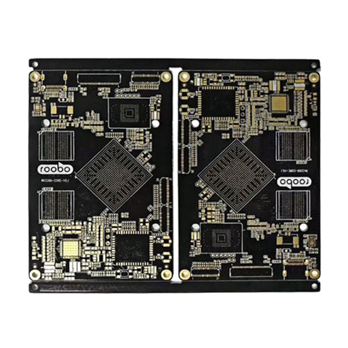
Blind and buried via technologies are integral to HDI PCBs, RF front-end modules, 5G communication boards, and high-speed computing backplanes. They support dense component placement, improve signal paths, and reduce overall board thickness.
Designers must carefully consider DFM (Design for Manufacturability) constraints, such as via aspect ratios, copper thickness uniformity, and dielectric material properties (Dk/Df). Collaboration between PCB designers and fabricators is crucial to balance performance, yield, and cost.
5. Conclusion
Blind and buried vias are no longer niche technologies—they are essential enablers of next-generation electronic miniaturization. When properly designed and fabricated, they deliver superior electrical characteristics and enable highly integrated, compact electronic systems.
