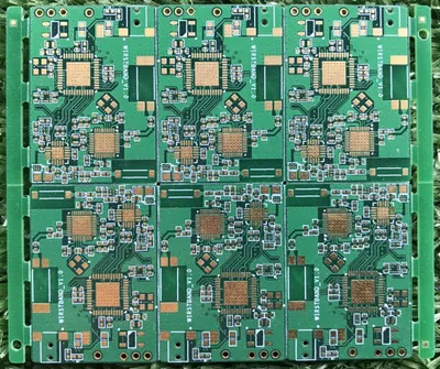
As high-frequency PCB design becomes increasingly prevalent in RF, 5G, and high-speed digital systems, the use of RO4350B PCB materials in combination with standard FR4 has led to the widespread adoption of hybrid PCB stackup design. A RO4350B hybrid stackup PCB enables designers to balance cost efficiency and high-frequency performance, making it ideal for complex RF PCB and mixed-signal applications.
However, RO4350B PCB hybrid stackup design introduces significant lamination challenges in mass production, including material compatibility, thermal mismatch, and process control. Understanding these challenges is essential for achieving reliable multilayer PCB manufacturing.
What Is RO4350B Hybrid Stackup Design?
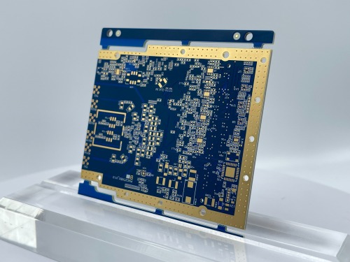
A RO4350B hybrid PCB stackup combines RO4350B high-frequency laminates with conventional FR4 materials within a multilayer PCB structure. This hybrid approach allows critical RF layers to benefit from low-loss PCB materials, while non-critical layers use cost-effective substrates.
Typical structure:
- RF signal layers using RO4350B laminates
- Digital/control layers using FR4
- Shared ground and power planes
This configuration is widely used in high-frequency PCB design and RF module PCB applications.
Advantages of RO4350B Hybrid PCB Stackup
- Reduced cost compared to full Rogers PCB stackups
- Excellent signal integrity in RF PCB design
- Improved low-loss transmission for high-frequency signals
- Flexibility in multilayer PCB layout design
- Compatibility with standard PCB fabrication processes
Key Design Considerations for RO4350B Hybrid Stackup
1. Controlled Impedance Across Different Materials
Maintaining controlled impedance in hybrid PCB design is challenging due to varying dielectric constants.
Key considerations:
- Adjust trace width for different layers
- Use precise impedance calculation tools
- Ensure consistent PCB stack-up design
2. Material Compatibility
RO4350B laminates and FR4 have different:
- Coefficient of thermal expansion (CTE)
- Dielectric properties
- Mechanical characteristics
Proper material selection is critical for hybrid PCB reliability.
3. Layer Alignment and Registration
Accurate alignment is essential in multilayer PCB lamination.
Misalignment can lead to:
- Impedance variation
- Signal integrity issues
- Manufacturing defects
4. Via Design in Hybrid PCB
Via structures crossing different materials can introduce stress and reliability risks.
Best practices:
- Optimize via aspect ratio
- Use back drilling to remove stubs
- Minimize transitions between materials
Lamination Challenges in Mass Production
1. Thermal Expansion Mismatch
One of the biggest challenges in RO4350B hybrid PCB lamination is the difference in CTE between RO4350B and FR4.
Impact:
- Delamination risk
- Barrel cracking in vias
- Warpage during reflow
2. Resin Flow Control
During lamination, resin flow behavior differs between materials.
Issues include:
- Voids and poor bonding
- Uneven dielectric thickness
- Delamination between layers
3. Lamination Temperature Profile Optimization
RO4350B PCB lamination requires precise temperature control.
Challenges:
- Different curing temperatures for RO4350B and FR4
- Risk of over-curing or under-curing
- Maintaining consistent pressure and heating rates
4. Drilling and Hole Quality
Hybrid materials affect PCB drilling performance.
Potential problems:
- Rough hole walls
- Smearing between layers
- Reduced plating quality
5. Warpage and Dimensional Stability
Hybrid PCB structures are prone to warpage due to uneven material properties.
Solutions:
- Symmetrical stack-up design
- Balanced copper distribution
- Controlled cooling processes
Process Optimization for Mass Production
1. Stack-Up Symmetry Design
Design symmetrical multilayer PCB stackups to reduce stress and improve stability.
2. Controlled Lamination Process
- Optimize pressure and temperature profiles
- Use compatible prepreg materials
- Monitor resin flow behavior
3. Advanced Drilling and Plating Techniques
Improve via reliability with:
- Laser drilling for microvias
- Controlled desmear processes
- Uniform copper plating
4. Quality Control and Testing
Ensure RO4350B PCB reliability through:
- Cross-section analysis
- Thermal cycling tests
- Impedance testing
Applications of RO4350B Hybrid PCB Stackup
- 5G communication modules
- RF transceivers and antennas
- Automotive radar systems
- High-speed networking equipment
- Mixed-signal PCB systems
These applications require both high-frequency performance and cost-effective PCB manufacturing.
Conclusion
RO4350B PCB hybrid stackup design provides an effective balance between performance and cost in high-frequency PCB applications. However, lamination challenges in mass production—such as thermal mismatch, resin flow control, and drilling complexity—must be carefully managed.
By optimizing PCB stack-up design, lamination processes, and material selection, manufacturers can achieve reliable, high-performance RO4350B hybrid PCBs suitable for demanding RF and high-speed applications.
