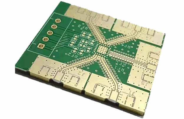
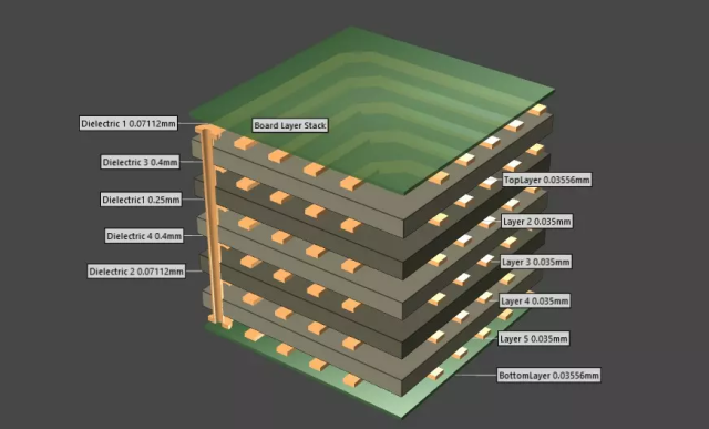
A PCB Layer Stackup refers to the arrangement of conductive copper layers and insulating dielectric materials that make up a multilayer PCB. In the era of high-speed digital electronics and 5G, the stackup is no longer just a mechanical carrier; it is a critical tool for managing signal integrity, power distribution, and electromagnetic compatibility (EMC). A well-engineered stackup from KKPCB ensures that your device operates without interference while maintaining structural durability.
1. Anatomy of a Layer Stackup
A typical multilayer board consists of three primary material types:
- Core: A rigid, pre-cured fiberglass-epoxy (FR-4) substrate with copper foil bonded to both sides.
- Prepreg: “Pre-impregnated” fiberglass layers that are uncured. These act as the “glue” that bonds the cores together during the PCB lamination process.
- Copper Foil: The conductive paths used for signal routing, power planes, and ground planes.
2. Types of Layers in a Stackup
- Signal Layers: The layers where electrical components are connected and high-speed data is routed.
- Ground Planes (GND): Solid copper planes that provide a return path for signals and shield against EMI.
- Power Planes (VCC): Dedicated layers for distributing stable voltage to various components across the board.
3. Why is Stackup Design Critical?
- Controlled Impedance: By precisely managing the thickness of the dielectric and the width of the traces, designers can achieve the specific impedance (e.g., 50Ω or 100Ω) required for high-speed signals.
- EMI Reduction: A balanced stackup with adjacent signal and ground layers minimizes the “loop area,” significantly reducing electromagnetic radiation and susceptibility.
- Thermal Management: Solid copper planes help spread heat generated by high-power components, preventing localized hot spots.
- Warpage Prevention: A symmetrical stackup (where the materials above and below the center are identical) is essential to prevent the board from bowing or twisting during the high-temperature reflow soldering process.
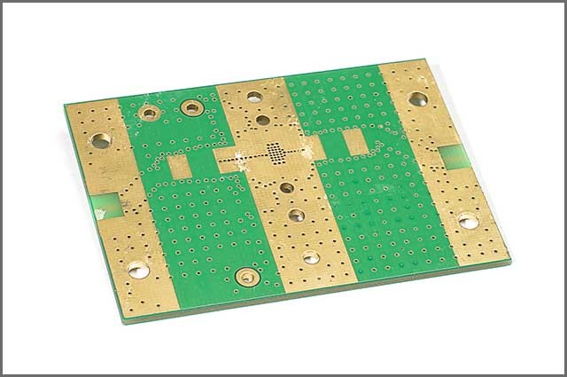
4. Common Stackup Configurations
- 4-Layer Stackup: Usually Signal—GND—Power—Signal. This is the entry-point for managing EMI more effectively than double-sided boards.
- 6-Layer Stackup: Adds two additional signal or plane layers, offering much better isolation for sensitive analog signals or high-speed traces.
- 8+ Layer Stackup: Used in complex High-Density Interconnect (HDI) designs, such as motherboards and servers, where multiple ground planes are needed to isolate high-speed differential pairs.
5. KKPCB’s Engineering Support
At KKPCB, we provide expert DFM (Design for Manufacturing) feedback on your stackup. We help you select the right materials (such as Rogers, Isola, or Panasonic MEGTRON) and calculate the exact dielectric thicknesses to ensure your controlled impedance targets are met on the first production run.
