
Power supply circuits are essential components in almost every electronic system, providing stable and reliable energy conversion for different functional modules. From consumer electronics and industrial equipment to automotive systems and renewable energy applications, the performance of the power supply PCB directly affects overall product reliability.
Compared with ordinary signal PCBs, power supply PCB design faces more demanding challenges, including:
- High current transmission
- Voltage conversion efficiency
- Heat generation
- Electromagnetic interference (EMI)
- Electrical safety requirements
Improper PCB design may result in:
- Excessive voltage drop
- Component overheating
- Power instability
- Electromagnetic interference
- Premature product failure
Therefore, engineers must consider electrical, thermal, mechanical, and manufacturing factors during the PCB design process.
This article introduces five key points in PCB design for power supply applications to help improve reliability and performance.
1. Optimize Current Carrying Capability and Power Trace Design
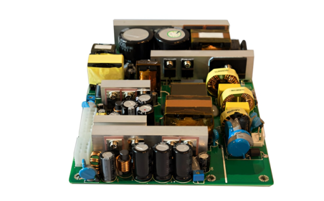
The primary function of a power supply PCB is to deliver electrical energy efficiently. Therefore, current carrying capability is one of the most important design considerations.
High current paths require careful optimization of:
- Trace width
- Copper thickness
- Layer selection
- Via structure
Trace Width Selection
Power traces should be designed according to:
- Maximum operating current
- Allowable temperature rise
- Copper thickness
- PCB material characteristics
Insufficient trace width can cause:
- Excessive resistance
- Voltage drop
- Heat accumulation
- Potential PCB damage
For high-current applications, designers may use:
- Wider copper traces
- Multiple copper layers
- Heavy copper PCB technology
Minimize Current Loop Area
High-current switching loops generate electromagnetic radiation.
To reduce EMI:
- Keep input/output current paths compact
- Minimize the distance between switching components
- Place power components close together
A smaller current loop reduces unwanted electromagnetic coupling and improves system stability.
2. Pay Attention to Thermal Management
Power supply circuits often generate significant heat due to:
- Switching losses
- Conduction losses
- Component resistance
- Power conversion inefficiency
Effective thermal management is essential for maintaining long-term reliability.
Component Placement for Heat Dissipation
High-power components such as:
- MOSFETs
- Transformers
- Inductors
- Power ICs
- Rectifiers
should be strategically positioned to prevent heat concentration.
Recommended practices include:
- Avoid placing heat-sensitive components near power devices
- Provide sufficient spacing between high-temperature components
- Create effective heat dissipation paths
Use Thermal Vias and Copper Areas
Thermal vias help transfer heat between PCB layers.
Additional methods include:
- Increasing copper area
- Using thicker copper layers
- Connecting thermal pads to ground planes
- Adding heat sinks when necessary
Good thermal design improves component lifespan and system reliability.
3. Improve Power Integrity and Voltage Stability
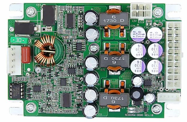
Power integrity determines whether the PCB can provide stable voltage and current to different system modules.
Poor power integrity may cause:
- Voltage fluctuations
- System resets
- Signal errors
- Reduced component performance
Optimize Power Distribution Network (PDN)
A reliable PDN should provide:
- Low impedance power delivery
- Stable voltage levels
- Reduced noise
Key design considerations include:
- Proper power plane design
- Short power connections
- Suitable capacitor selection
- Low-inductance return paths
Decoupling Capacitor Placement
Decoupling capacitors should be placed:
- Close to IC power pins
- With short connection traces
- With direct grounding paths
This helps suppress high-frequency noise and transient current demands.
4. Control EMI and EMC Performance
Power supply circuits, especially switching power supplies, are common sources of electromagnetic interference.
High-frequency switching currents may generate:
- Radiated emissions
- Conducted noise
- Crosstalk with sensitive circuits
Reduce Switching Noise
Important design methods include:
Minimize Switching Loop Area
The high-frequency switching loop should be as small as possible.
Separate Power and Sensitive Circuits
Keep switching regulators away from:
- Analog circuits
- RF circuits
- Sensor interfaces
- Communication modules
Optimize Grounding
A proper grounding structure helps:
- Reduce noise coupling
- Improve signal integrity
- Control EMI emissions
Add Filtering and Shielding When Required
Depending on application requirements, designers may use:
- EMI filters
- Common-mode chokes
- Shielding structures
- Ground barriers
These methods help improve EMC performance and support compliance with industry standards.
5. Consider Electrical Safety and Manufacturing Requirements
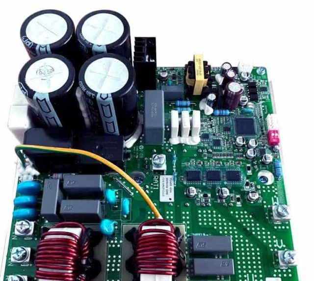
Power supply PCBs often involve high voltages, requiring careful attention to safety design.
Maintain Proper Clearance and Creepage Distance
High-voltage designs require sufficient spacing between conductive areas.
Important factors include:
- Operating voltage
- Pollution degree
- Material properties
- Safety standards
Insufficient spacing may lead to:
- Electrical arcing
- Insulation breakdown
- Safety risks
PCB Material Selection
The PCB material should match application requirements.
Important considerations include:
- Thermal performance
- Dielectric strength
- Mechanical stability
- Flame resistance
For demanding applications, materials with enhanced thermal and electrical properties may be required.
Manufacturing Considerations
Power supply PCB manufacturing should consider:
- Copper thickness consistency
- Via reliability
- Soldering quality
- Component assembly requirements
Design for Manufacturing (DFM) review can help identify potential production risks before fabrication.
Additional Considerations for Different Power Supply Applications
Different applications have different PCB design priorities.
Automotive Power Supply PCB
Important requirements:
- High reliability
- Thermal cycling resistance
- Vibration resistance
- EMC compliance
Industrial Power Supply PCB
Focus areas include:
- Long operating life
- High current capability
- Stable operation under harsh environments
High-Frequency Switching Power Supply PCB
Key concerns include:
- Switching noise control
- Power loop optimization
- EMI reduction
- High-speed current return paths
Common Power Supply PCB Design Mistakes
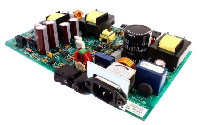
Several design issues frequently affect power supply performance:
- Using insufficient trace width for high current
- Ignoring thermal paths
- Poor placement of switching components
- Incorrect grounding strategy
- Long high-current loops
- Insufficient safety spacing
- Lack of EMI consideration
Avoiding these problems during the design stage can significantly improve product reliability.
Conclusion
Power supply PCB design requires a balance between electrical performance, thermal management, EMC control, safety requirements, and manufacturability.
The five key considerations include:
- Optimizing current paths and trace design
- Managing heat generation effectively
- Improving power integrity and voltage stability
- Controlling EMI and EMC performance
- Ensuring electrical safety and manufacturing reliability
By applying these principles during PCB development, engineers can create power supply boards with improved efficiency, stability, and long-term reliability for demanding electronic applications.
