
In PCB design, grounding is one of the most fundamental yet critical factors affecting electronic system performance. A well-designed grounding structure provides stable current return paths, reduces electrical noise, improves signal integrity, and enhances overall system reliability.
As electronic products continue moving toward higher speeds, greater integration, and smaller form factors, PCB grounding design has become increasingly challenging. High-speed digital signals, RF circuits, power electronics, and sensitive analog components all have different grounding requirements.
Poor grounding design can lead to various issues, including:
- Signal interference
- Increased electromagnetic interference (EMI)
- Voltage fluctuations
- Signal integrity degradation
- System instability
Therefore, grounding considerations should be integrated into PCB design from the early development stage rather than treated as a final optimization step.
1. Why Grounding Is Important in PCB Design
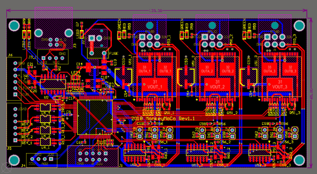
Grounding serves as a reference point for electrical circuits and provides a return path for current flow.
In an ideal PCB design, current should follow a predictable and low-impedance return path. However, at higher frequencies, current tends to follow the path with the lowest impedance rather than simply the shortest physical route.
A proper grounding design helps achieve:
Stable Voltage Reference
Sensitive circuits require a stable reference voltage. Ground noise or ground potential differences may affect measurement accuracy and system operation.
Improved Signal Integrity
High-speed signals rely on controlled current return paths. Poor grounding can introduce:
- Signal reflections
- Crosstalk
- Timing errors
- Increased transmission loss
Reduced EMI Problems
Uncontrolled current loops can generate electromagnetic radiation. Optimized grounding helps minimize unwanted noise emissions and improves EMC performance.
2. Selecting the Appropriate Grounding Structure
Different PCB applications require different grounding strategies.
2.1 Ground Plane Design
A continuous ground plane is one of the most effective methods for improving PCB electrical performance.
Advantages include:
- Lower return path impedance
- Reduced noise coupling
- Improved signal integrity
- Better EMI control
For multilayer PCBs, dedicated ground layers are commonly used to provide stable reference planes for high-speed signals.
2.2 Single-Point Grounding
Single-point grounding connects different circuit sections at one common location.
This method is often suitable for:
- Low-frequency analog circuits
- Audio systems
- Precision measurement equipment
However, it may not be ideal for high-speed circuits because long return paths can increase inductance.
2.3 Multi-Point Grounding
Multi-point grounding connects multiple ground locations to reduce impedance.
It is commonly applied in:
- High-frequency circuits
- RF systems
- Digital communication equipment
Proper implementation helps reduce ground noise and improve high-speed performance.
3. Grounding Considerations for Different PCB Applications
High-Speed Digital PCB Design
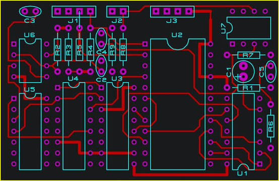
High-speed circuits require careful control of return current paths.
Important considerations include:
- Maintaining continuous reference planes
- Avoiding signal layer transitions without ground support
- Minimizing return path discontinuities
When high-speed signals cross split ground planes, current may be forced to take longer paths, causing impedance changes and EMI issues.
RF and Microwave PCB Design
RF circuits are highly sensitive to grounding quality.
Important design practices include:
- Maintaining solid ground areas
- Using sufficient ground vias
- Reducing parasitic inductance
- Optimizing transmission line structures
In RF applications, grounding directly affects:
- Signal loss
- Noise performance
- Radiation characteristics
- Impedance stability
Power Electronics PCB Design
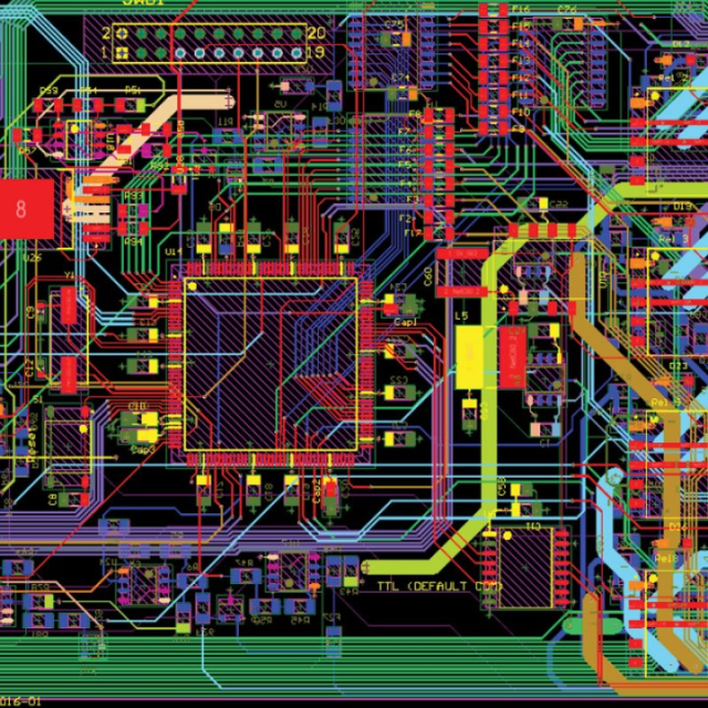
Power circuits involve high current switching, creating significant electrical noise.
Grounding design should consider:
- High-current return paths
- Separation between power and control grounds
- Minimizing ground loops
- Reducing switching noise
Proper grounding helps improve:
- Power efficiency
- Thermal performance
- System reliability
4. Common PCB Grounding Problems
4.1 Ground Loops
Ground loops occur when multiple grounding paths create unwanted circulating currents.
Potential consequences include:
- Noise increase
- Signal distortion
- Measurement errors
Proper grounding topology and layout planning help prevent these issues.
4.2 Improper Ground Plane Splitting
Although separating analog and digital grounds can sometimes be beneficial, unnecessary ground plane splits may create problems.
Issues include:
- Longer return current paths
- Increased EMI
- Signal integrity degradation
Ground separation should be based on current flow analysis rather than simply dividing different circuit sections.
4.3 Insufficient Ground Via Design
In multilayer PCBs, vias connect ground layers and provide return paths.
Insufficient ground vias may result in:
- Increased inductance
- Poor high-frequency performance
- EMI problems
Via placement should be carefully considered, especially near high-speed signals and RF components.
5. Grounding Design Optimization Methods
5.1 Keep Return Paths Short and Direct
A short return path reduces loop area and minimizes electromagnetic radiation.
Engineers should:
- Place decoupling capacitors close to power pins
- Maintain continuous ground planes
- Avoid unnecessary routing changes
5.2 Separate Noisy and Sensitive Circuits
High-noise circuits should be isolated from sensitive signal areas.
Examples include:
- Switching power supplies
- Motor control circuits
- RF transmit sections
Proper placement reduces unwanted interference.
5.3 Use Simulation and Verification Tools
For complex PCB designs, simulation can help evaluate grounding performance.
Common analysis methods include:
- Signal integrity simulation
- Power integrity analysis
- EMI simulation
Early verification helps identify potential grounding risks before manufacturing.
6. Manufacturing Impact of Grounding Design
Grounding design is not only an electrical consideration but also affects PCB manufacturability.
Key manufacturing factors include:
Copper Distribution
Uneven copper distribution may cause:
- PCB warpage
- Etching variation
- Manufacturing inconsistency
Layer Stack-Up
A balanced stack-up helps maintain:
- Mechanical stability
- Controlled impedance
- Reliable grounding performance
Surface Finish and Via Reliability
Reliable vias and surface connections are essential for maintaining stable grounding paths throughout product operation.
Conclusion
Grounding is a fundamental element of successful PCB design. From high-speed digital systems and RF circuits to power electronics and industrial applications, proper grounding directly influences signal integrity, EMI performance, and product reliability.
A successful grounding strategy requires careful consideration of circuit characteristics, current flow, PCB stack-up, material selection, and manufacturing capability.
By addressing grounding considerations during the early design stage, engineers can reduce development risks, improve system performance, and create more reliable PCB solutions for demanding electronic applications.
