
This guide explains how via in pad works, what VIPPO (via-in-pad plated over) means, which design rules to follow and how the process affects cost and assembly. The manufacturing values quoted come from KKPCB’s published PCB manufacturing capabilities.
1. Why Designers Use Via in Pad
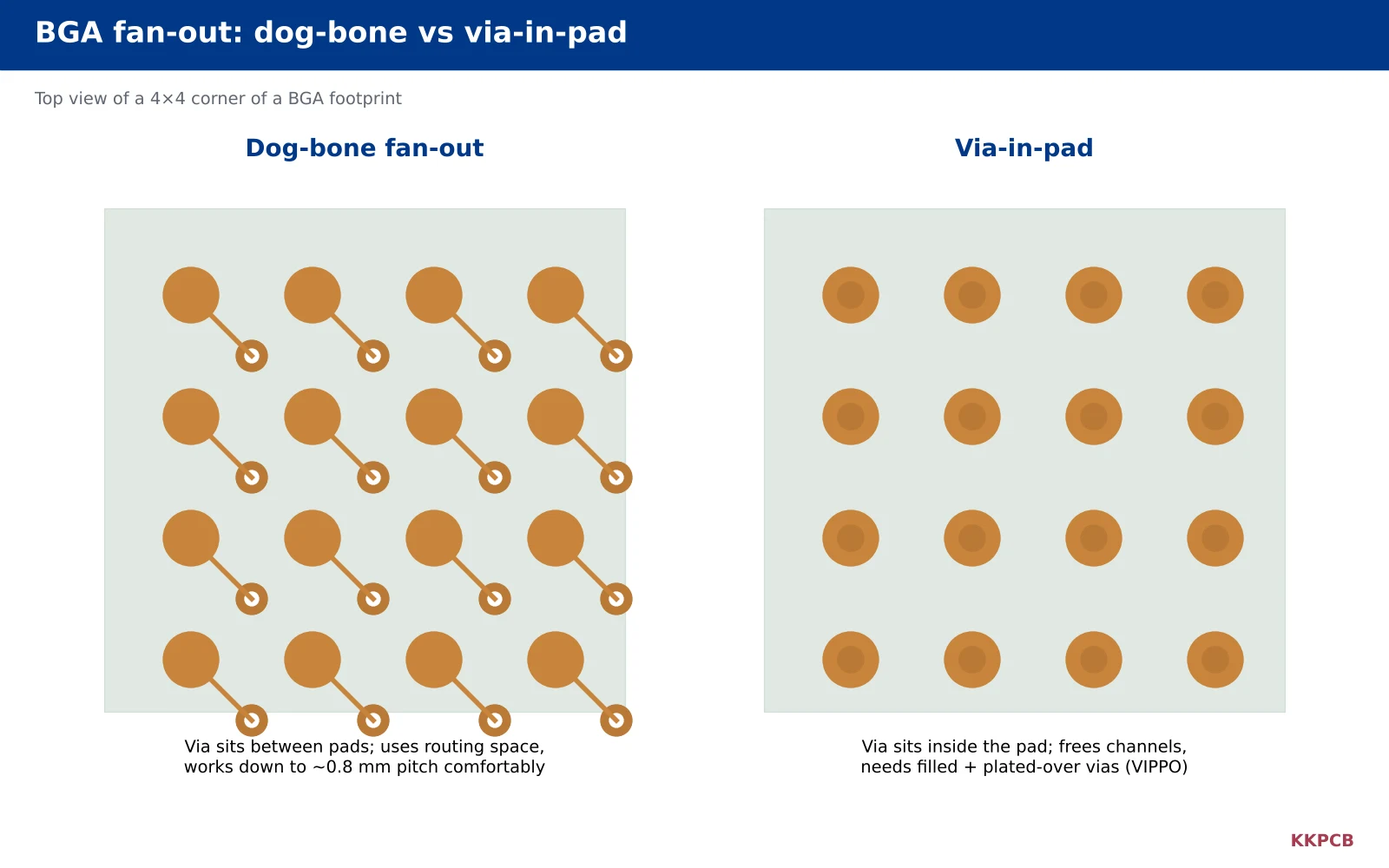
In a conventional “dog-bone” fan-out, each BGA pad connects through a short trace to a via placed between the pads. That works well while there is enough space between balls. As pitch shrinks, the space disappears:
- Fine-pitch BGA escape: at 0.5 mm pitch and below there is usually no room for a via between pads, so the via has to move into the pad.
- Freed routing channels: removing dog-bone vias opens space on the outer layer and on inner layers for more traces.
- Shorter, lower-inductance connections: a via directly under the pad shortens the path to power and ground planes, which helps decoupling and high-speed signals.
- Thermal performance: vias in a thermal pad move heat into inner planes or to the opposite side of the board.
2. What Is VIPPO?
VIPPO stands for via-in-pad plated over. It describes the complete process that makes a via in a pad safe for soldering: the hole is plated, filled, planarized flat and then plated over with copper so that the surface finish is applied to a continuous metal pad.
In IPC-4761, the standard that classifies via protection methods, this construction corresponds to a filled and capped via (Type VII). Referencing the standard on the fabrication drawing removes ambiguity about what is expected.
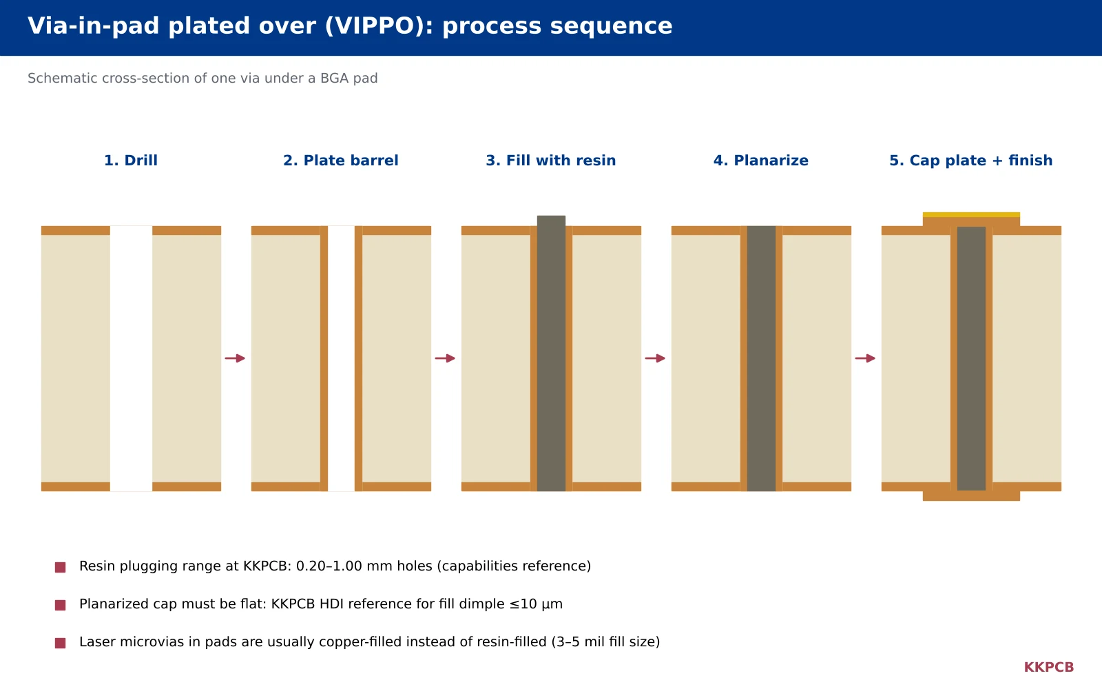
The VIPPO process step by step
- Drill the via holes that will sit in pads.
- Plate the barrel to the required copper thickness.
- Fill the hole, usually with a non-conductive epoxy resin.
- Planarize by grinding or brushing the surface flat so no resin protrudes and no dimple remains.
- Cap plate copper over the filled via, then image, etch and apply the surface finish.
3. Resin Fill, Copper Fill and Conductive Fill
| Fill type | Typical use | Notes |
|---|---|---|
| Non-conductive epoxy (resin plugging) | Mechanically drilled vias in BGA and component pads | Most common VIPPO method. KKPCB resin-plugged hole range: 0.20–1.00 mm. |
| Copper fill plating | Laser microvias in HDI pads, stacked microvias | Microvia becomes solid copper. KKPCB HDI reference: 3–5 mil fill size, dimple ≤10 µm. |
| Conductive epoxy | Selected thermal or current paths | Thermal benefit depends mostly on the plated barrel; CTE behaviour of the paste must be reviewed. |
For most mechanically drilled vias, a non-conductive resin fill with a copper cap is the standard choice. The electrical and most of the thermal conduction happen through the plated copper barrel, so a conductive paste is rarely necessary. Laser microvias in HDI designs are normally copper-filled, which is also what allows them to be stacked; see any-layer HDI PCB for that construction.
4. What Happens If the Via Is Left Open
Placing an unfilled via in a pad is a common and costly mistake. During reflow, molten solder is drawn into the open hole by capillary action. The consequences include:
- Insufficient solder left on the pad, leading to weak or open BGA joints.
- Voids caused by air and flux volatiles escaping from the via during reflow.
- Solder on the opposite side of the board, which can interfere with components or test points.
- Inconsistent results that pass first-article inspection but fail on a later production lot.
Tenting the via with solder mask is not a substitute inside a pad, because the pad itself must be open to solder.
5. Via-in-Pad Design Rules
Mark VIPPO vias clearly
Use a separate drill file or a clearly defined drill symbol for vias that must be filled and capped. Fabricators process filled vias in a different sequence from other holes, and ambiguous data is the most frequent cause of engineering questions.
Keep hole sizes inside the fill window
Design VIPPO holes within the fabricator’s resin-plugging range. At KKPCB the reference range is 0.20–1.00 mm. Very small mechanical holes in thick boards also raise the PCB aspect ratio, which affects plating quality.
Account for extra surface copper
Cap plating adds copper to the outer layers. Fine traces on those layers must be designed for the final copper thickness, not just the starting foil. KKPCB’s outer-layer line/space values by copper weight are listed on the capabilities page.
Specify flatness
State the acceptable dimple or protrusion over the filled via. KKPCB’s HDI reference for hole-fill dimple is 10 µm or less, which supports fine-pitch stencil printing.
Choose a flat surface finish
VIPPO pads are usually finished with ENIG, ENEPIG or OSP. A domed solder finish defeats much of the benefit; see our comparison of HASL vs ENIG.
Thermal pads
For QFN and power package thermal pads, a full VIPPO treatment is not always required. Alternatives include small plugged vias or a windowed paste pattern, but the decision should be agreed with your assembler because it affects voiding.
6. Cost Impact of Via in Pad
VIPPO adds process steps: resin filling, curing, planarization and an additional plating cycle. It therefore increases the bare-board price and lead time compared with dog-bone fan-out. The cost is usually justified when:
- the BGA pitch makes dog-bone fan-out impossible,
- using via in pad avoids extra layers or a larger board, or
- electrical or thermal performance clearly requires it.
If only a few pads need it, discuss whether the rest of the board can use conventional vias to keep cost under control.
7. Assembly Considerations
- Stencil design: with properly filled and capped vias, stencil apertures can follow normal pad rules.
- X-ray inspection: BGA joints over VIPPO pads should be checked for voiding and wetting, as for any BGA.
- Reflow profile: the profile must suit the component and board thermal mass, especially where many vias connect pads to large planes.
Our BGA PCB assembly process includes X-ray inspection for hidden joints.
8. How Filled Vias Are Inspected and Accepted
Because a filled and capped via is hidden under copper and surface finish, its quality has to be verified by process control and destructive sampling rather than visual inspection alone. A typical verification plan includes:
- Microsection analysis of coupons or sample boards to check that the fill is complete, free of significant voids, and bonded to the barrel wall.
- Cap plating thickness measured on the microsection, together with the barrel copper underneath.
- Planarity of the capped surface – the dimple or protrusion over the via – against the agreed limit.
- Thermal stress testing that simulates the reflow profile, followed by a second microsection to confirm that the cap has not separated from the fill or the barrel.
Defects to look for include voids in the resin, cracks between the cap plating and the barrel, and resin recession that leaves a dimple under the surface finish. Agreeing the inspection points and sample size before production avoids disputes about acceptance later.
9. Via-in-Pad Design Checklist
Use this checklist before releasing a design with via in pad:
| Check | Why it matters |
|---|---|
| Every via in a solderable pad is marked as filled and capped | Prevents solder wicking and voids |
| VIPPO holes have their own drill file or symbol | The fabricator processes them in a separate sequence |
| Hole sizes are within the resin-plug range (0.20–1.00 mm at KKPCB) | Holes outside the range may not fill reliably |
| Aspect ratio of each VIPPO hole has been checked | Plating must reach the middle of the barrel before filling |
| Outer-layer traces are sized for final copper after cap plating | Extra copper affects minimum line/space |
| Surface finish is flat (ENIG, ENEPIG or OSP) | Domed finishes undo the benefit of planarization |
| Planarity requirement stated on the drawing | Supports fine-pitch stencil printing |
| Assembler has reviewed stencil and X-ray plan | Confirms the assembly side is ready for VIPPO pads |
10. Via in Pad vs Other Fan-Out Options
Via in pad is one of several ways to escape a dense component. Dog-bone fan-out remains the lowest-cost option where it fits. Laser microvias in pads, copper-filled, are the standard approach in HDI designs and avoid mechanical holes on the outer layers altogether. Mechanically drilled VIPPO is the usual choice on thicker multilayer boards where laser microvias are not used. Comparing these options at the stack-up stage – rather than after placement – gives the widest choice and the clearest cost picture.
11. Via in Pad for Power and Thermal Pads
Power devices such as QFN regulators, MOSFETs in surface-mount packages and LED drivers often have a large exposed pad that must conduct heat into the board. Vias in that pad are effective because they shorten the path to inner ground or power planes, which act as heat spreaders. Several design choices affect how well this works:
- Via count and diameter: heat flows mainly through the plated copper barrel, so several smaller vias usually conduct more heat than one large via of the same total area.
- Connection to planes: vias should connect solidly to inner copper planes; thermal-relief spokes reduce heat flow.
- Filled or open: filled and capped vias give a flat pad and predictable solder volume. Small open vias can be acceptable in some thermal pads if the paste pattern is designed for them, but this must be agreed with the assembler.
- Copper weight: heavier inner copper spreads heat better; see our heavy copper PCB options.
Frequently Asked Questions
Is via in pad the same as VIPPO?
Via in pad describes the layout choice of putting a via inside a pad. VIPPO describes the manufacturing treatment that makes it solderable: filling, planarizing and plating over the via. A via in pad intended for soldering should normally be VIPPO.
At what BGA pitch do I need via in pad?
Many designs move to via in pad at 0.5 mm pitch or below, where dog-bone fan-out no longer fits. Larger-pitch BGAs may still use it to save routing space or improve power delivery.
Can I use via in pad without filling the via?
For pads that will be soldered, this is not recommended. Solder wicks into the open hole, causing voids or insufficient joints. Unfilled vias in pads are only acceptable in special cases agreed with the fabricator and assembler.
Does VIPPO increase PCB cost?
Yes. Filling, planarizing and cap plating add process steps and time. The increase is often justified by eliminating layers, enabling fine-pitch BGAs or improving yield.
What should I write on the fabrication drawing?
Identify which vias are filled and capped, reference IPC-4761 Type VII if appropriate, specify the fill material, planarity requirement and surface finish, and supply a separate drill file for the VIPPO holes.
Build Your Via-in-Pad Design with KKPCB
KKPCB supports resin-plugged and copper-filled via-in-pad structures on multilayer and HDI PCB builds, and reviews every VIPPO request against drill size, board thickness and finish. Our DfMA services can check your fan-out strategy before layout is frozen.
Designing a fine-pitch BGA board? Contact KKPCB to review your via-in-pad requirements.
PCB fabrication at KKPCB follows the acceptance criteria of IPC (IPC-6012, IPC-A-600).