
That routing freedom has a price. An any-layer board needs more sequential lamination cycles, tighter registration and more copper-fill plating than a conventional HDI PCB, so the decision should be made deliberately. This guide explains how any-layer HDI is built, when it is worth the cost, which design rules matter and what manufacturing data you should check before release.
1. What Is an Any-Layer HDI PCB?
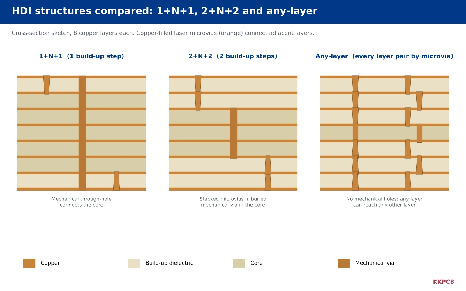
HDI boards are usually described with a build-up notation such as 1+N+1 or 2+N+2. The “N” is a conventional multilayer core, and each number on the outside is one laser-drilled build-up step added on each side of that core.
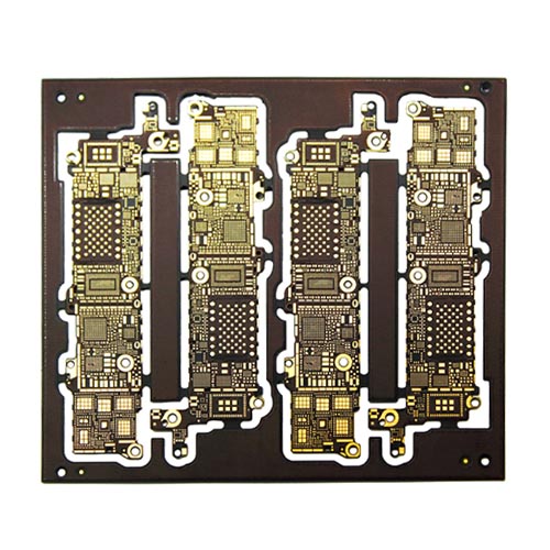
An any-layer HDI PCB – also called ELIC (every layer interconnect) – removes the conventional core as a routing barrier. Each dielectric layer is laser-drilled and the microvias are filled with copper, so microvias can be stacked directly on top of each other through the full thickness of the board.
- 1+N+1: one microvia layer on each side, with the core connected by mechanical drilling.
- 2+N+2 / 3+N+3: two or three build-up steps per side, often with stacked or staggered microvias and a buried mechanical via in the core.
- Any-layer: every layer pair is connected by laser microvias, so the routing engineer can drop from L1 to L6, or jump from L3 to L4, at almost any location.
2. When Does an Any-Layer HDI PCB Make Sense?
Any-layer HDI is not automatically “better” than a 2+N+2 or 3+N+3 structure. It solves specific problems, and it should be justified by at least one of them.
Very dense BGA escape
Fine-pitch processors, memory and RF transceivers can have hundreds of balls in a small area. When the pitch is small enough that a via cannot fit between pads, the via has to be placed in the pad and routed out through several inner layers. Any-layer HDI lets each ring of balls escape on a different layer without consuming board area for through-holes. KKPCB’s HDI capability reference lists a minimum BGA centre-to-centre distance of 0.3 mm, which should be checked against your package before layout starts.
Board area is fixed by the enclosure
In phones, earbuds, smart watches and camera modules, the board outline is defined by the product, not by the PCB designer. Removing through-holes frees space on every layer, which can be enough to avoid adding layers or making the board larger.
Short, controlled vertical transitions
Stacked microvias create short vertical paths with small stubs. For high-speed digital interfaces this can help, although the benefit must be confirmed by simulation and impedance control on the actual stack-up.
When not to choose it
If your BGA pitch allows dog-bone fan-out, if the board is large, or if cost is the primary driver, a 1+N+1 or 2+N+2 structure is normally the more economical choice. Many industrial and automotive boards are better served by a robust multilayer PCB with a limited number of laser microvias.
3. How an Any-Layer HDI PCB Is Manufactured
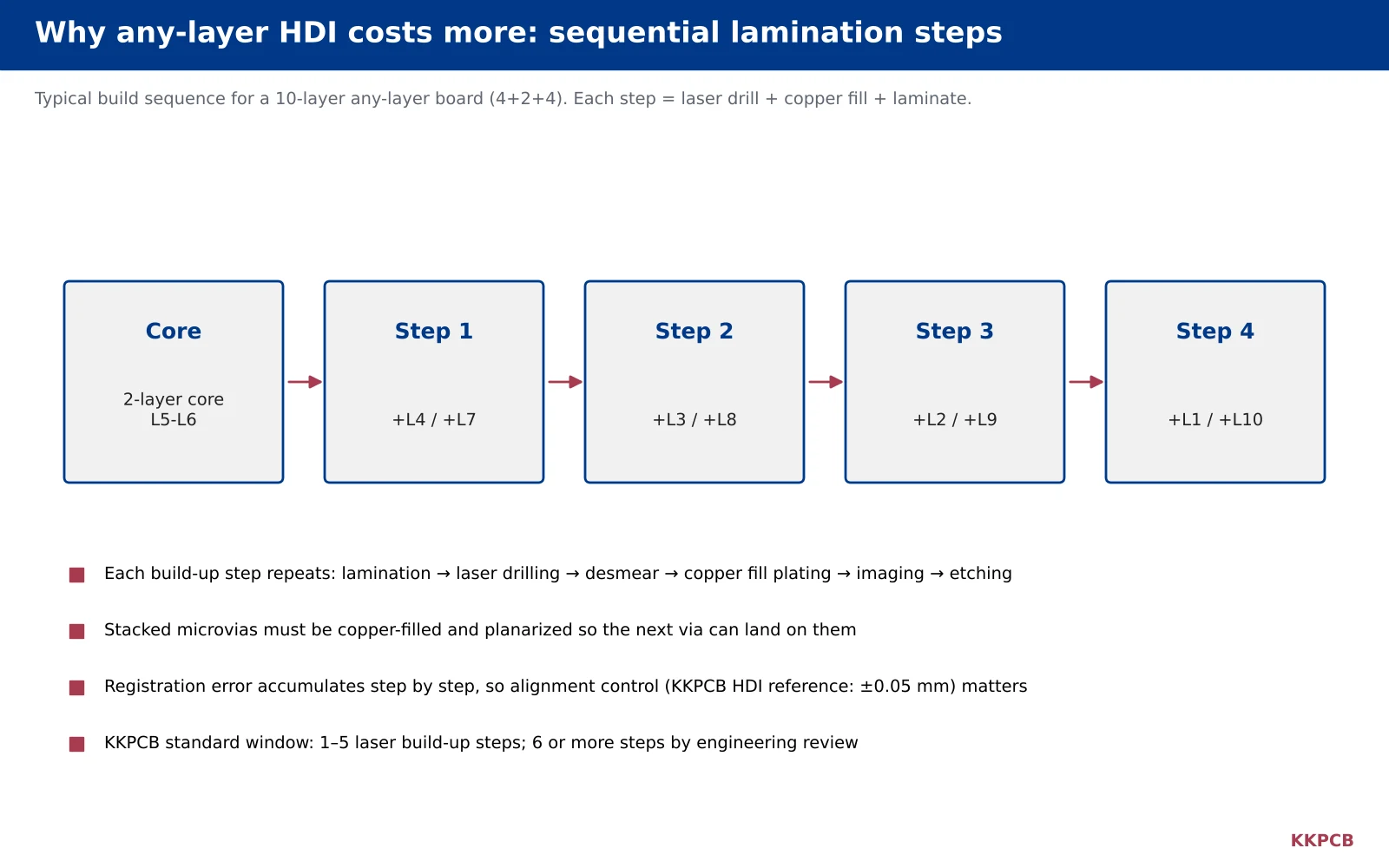
The defining feature of any-layer HDI is sequential lamination. The board is built from the centre outwards, and every build-up step repeats the same set of processes.
The build-up cycle
- Lamination of a thin dielectric and copper foil onto the existing sub-assembly.
- Laser drilling of microvias down to the copper pad of the layer below.
- Desmear and metallization so copper can adhere to the via wall.
- Copper fill plating so the microvia becomes solid and flat enough for the next via to land on top.
- Imaging and etching of the new outer layer before the next cycle begins.
A 10-layer any-layer board is commonly built as 4+2+4: a two-layer core plus four build-up steps on each side. Each step adds handling, lamination stress and registration tolerance, which is why the number of steps drives both cost and yield.
Copper-filled, stacked microvias
Stacked microvias only work when each via is completely filled and planarized. A dimple or void in a lower via becomes a weak point for the via landing on top of it. KKPCB’s HDI capability table lists via-fill electroplating for 3–5 mil microvias and a hole-fill dimple specification of 10 µm or less.
Registration across many lamination cycles
Every lamination cycle introduces small dimensional movement. The laser must hit the capture pad on the layer below, cycle after cycle. KKPCB’s HDI reference values include laser drilling accuracy of 0.025 mm and interlayer alignment of ±0.05 mm.
4. Key Design Rules for an Any-Layer HDI PCB
The table below summarizes the main parameters to agree with your fabricator. The KKPCB values come from the PCB manufacturing capabilities and HDI capabilities pages; extreme values must still be confirmed in engineering review.
| Parameter | KKPCB reference | Design note |
|---|---|---|
| HDI construction | 1–5 laser build-up steps; any-layer available; 6 or more steps by review | Confirm the step count before routing, not after. |
| Layer count | 1–40 layers; above 30 by review | Most any-layer designs are far below this limit. |
| Laser hole | 0.075–0.10 mm (4 mil standard, 3 mil by review) | Smaller holes reduce pad size but tighten plating control. |
| Laser hole vs depth | 0.10 mm for depth ≤55 µm; 0.13 mm for depth ≤100 µm | Choose dielectric thickness and hole size together. |
| Minimum line / space | 2/2 mil prototype; 3/3 mil volume (0.5 oz inner layers) | Plan volume production on the volume column. |
| Minimum core / prepreg | 2 mil | Thin dielectrics affect impedance and handling. |
| Microvia fill | Copper fill 3–5 mil; dimple ≤10 µm | Required for stacked vias and via-in-pad. |
| Controlled impedance | ±5 Ω below 50 Ω; ±10% at or above 50 Ω | Share target impedances with the stack-up request. |
Practical layout guidelines
- Keep stacks straight where possible. Stacked microvias save space; staggered microvias spread stress. Discuss with the fabricator which layers may be stacked and how many vias high.
- Use symmetric build-up. An unbalanced copper distribution or dielectric thickness increases warpage across many lamination cycles.
- Define capture-pad sizes early. Pad size must allow for laser accuracy and layer-to-layer registration.
- Do not mix finishes casually. Fine-pitch pads normally need a flat finish such as ENIG or OSP; see our PCB surface finishes guide.
- Plan test access. Dense boards leave little room for test points, so agree the electrical test and assembly inspection strategy at the same time as the layout.
5. Cost Drivers of an Any-Layer HDI PCB
Any-layer HDI is priced mainly by process steps rather than by board area. The main drivers are:
- Number of build-up steps: every step repeats lamination, laser drilling, plating and imaging.
- Copper-fill plating: filling and planarizing microvias is slower than standard plating.
- Yield risk: a defect in an early step affects every layer built on top of it.
- Material: thin, laser-drillable dielectrics and low-profile copper foils cost more than standard FR-4 cores.
- Finish and fine features: very fine line/space and selective finishes add inspection and process time.
A useful exercise before committing to any-layer HDI is to ask your fabricator to quote two stack-ups: an any-layer version and a 2+N+2 or 3+N+3 alternative. In many designs the alternative only needs a few local layout changes and saves several build-up cycles.
6. Any-Layer HDI PCB Reliability and Inspection
Because an any-layer HDI PCB is a stack of many thin, laminated layers, reliability depends on the interface between each microvia and its target pad. Typical controls include:
- Microsection analysis of stacked microvias to check fill, plating thickness and interface quality.
- Automated optical inspection of fine lines on each layer before the next lamination.
- X-ray checks of layer registration and via landing.
- Impedance coupons measured by TDR when controlled impedance is specified.
- Thermal stress testing that reflects the assembly profile, including lead-free reflow.
KKPCB builds to IPC Class 2 and Class 3 acceptance criteria, and the inspection plan should be agreed for the required class before production. More information on our process controls is available on the quality control page.
7. A Practical Workflow for Any-Layer HDI Projects
Any-layer HDI projects succeed when the stack-up is agreed before routing. A workflow that avoids most late changes looks like this:
- Share the component data first. Send the BGA pitch, ball count and escape requirements together with the target board thickness.
- Agree the build-up structure. Decide whether the design needs true any-layer or whether a 2+N+2 or 3+N+3 structure with local stacked vias is enough.
- Freeze the stack-up. Confirm dielectric thicknesses, copper weights, impedance targets and the via spans permitted on each layer pair.
- Route against the agreed rules. Use the confirmed laser hole, capture pad and line/space values in the design rules of your CAD tool.
- Run a DFM check before release. A fabricator review catches unsupported via spans, insufficient capture pads and copper imbalance before tooling.
- Build a prototype with full inspection. Microsections and impedance coupons from the first build confirm that the stack-up behaves as modelled.
KKPCB’s DfMA services can support steps 2, 3 and 5.
8. Any-Layer HDI vs 2+N+2: Quick Comparison
| Aspect | 2+N+2 HDI | Any-layer HDI |
|---|---|---|
| Routing freedom | High on the outer build-up layers; limited through the core | Highest: any layer to any layer |
| Mechanical drilling | Core and through-holes | Usually none, or only for special features |
| Lamination cycles | Fewer | More: one per build-up step |
| Typical applications | Tablets, industrial controllers, automotive electronics | Smartphones, wearables, camera and RF modules |
| Relative cost | Lower | Higher |
For a deeper look at blind and buried via rules, see Blind and Buried Vias in HDI PCB. If your design places vias directly inside BGA pads, our guide to via in pad (VIPPO) explains the filling and plating requirements.
Frequently Asked Questions
Is any-layer HDI the same as ELIC?
Yes. ELIC stands for “every layer interconnect” and describes the same idea: every layer pair is connected by stacked, copper-filled laser microvias, so the design does not depend on mechanically drilled holes through the core.
How many layers can an any-layer HDI PCB have?
The layer count is limited mainly by the number of build-up steps. KKPCB’s standard window is 1–5 laser build-up steps, which covers common any-layer constructions such as 8 and 10 layers; designs that need six or more steps are reviewed case by case.
What laser via size should I design for?
Start from 0.10 mm (4 mil) laser holes, which are standard at KKPCB. Smaller 0.075 mm (3 mil) holes are possible by review, but they must be matched to a thinner dielectric so that the via can still be plated and filled reliably.
Can any-layer HDI be combined with high-frequency materials?
It can, but laser drilling, desmear and copper fill must suit the chosen dielectric. Mixed constructions should be reviewed early; our high-frequency PCB team can advise on material compatibility.
What files do I need for an any-layer HDI quotation?
Send Gerber or ODB++ data, the proposed stack-up with build-up notation, drill files for every laser and mechanical span, impedance requirements, surface finish, quantity and test requirements. Clear drill-span definitions avoid most quotation delays.
Work with KKPCB on Your Any-Layer HDI Project
KKPCB manufactures HDI boards from 1+N+1 to any-layer constructions, and supports the full path from PCB prototype to small and medium-volume production, including BGA PCB assembly. Our engineers can compare stack-up options and confirm the achievable build-up window before you release the layout.
Planning an any-layer HDI PCB? Contact KKPCB with your stack-up and BGA requirements for a DFM review.
PCB fabrication at KKPCB follows the acceptance criteria of IPC (IPC-6012, IPC-A-600).