
For Satellite PCB launch design, a Ku/Ka payload can meet its schematic targets and still lose margin at the board edge. The connector, launch pad, reference plane, via field, and enclosure datum form one electromagnetic interface. The Satellite PCB release must hold that board-to-enclosure datum constant across design and manufacturing. At 30 GHz, even a short discontinuity or an inconsistent ground return can become visible in channel-to-channel phase and amplitude. A Satellite PCB launch review should therefore start from the complete mechanical and electrical interface, not from the connector footprint alone.
Satellite PCB Launch Design: Treat the launch as a system interface
Start by fixing connector family, board-edge datum and stackup, plating, screw or clamp features, and the enclosure reference plane. A connector drawing may define its own recommended landing geometry, but the board stackup, finished copper, solder mask, edge tolerance, and chassis contact all affect the realized transition. When an RF module connects to a payload panel or test fixture, the connector pin map and return contacts should be reviewed together with the board outline and assembly access. Satellite PCB requirements are strongest when the mechanical model and released copper data use the same revision.
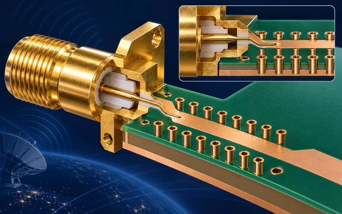
In Satellite PCB Launch Design, a surface-mount edge launch, the signal pad should meet the transmission line without an abrupt width step, while ground tabs need a low-inductance path into the reference structure. Avoid a large ground-plane setback or a copper neck that forces return current around a slot. If solder mask or edge plating changes near the launch, include it in the drawing and fabrication notes; undocumented “small” changes can shift the interface between prototypes and production.
Satellite PCB Launch Design: Keep the reference path continuous
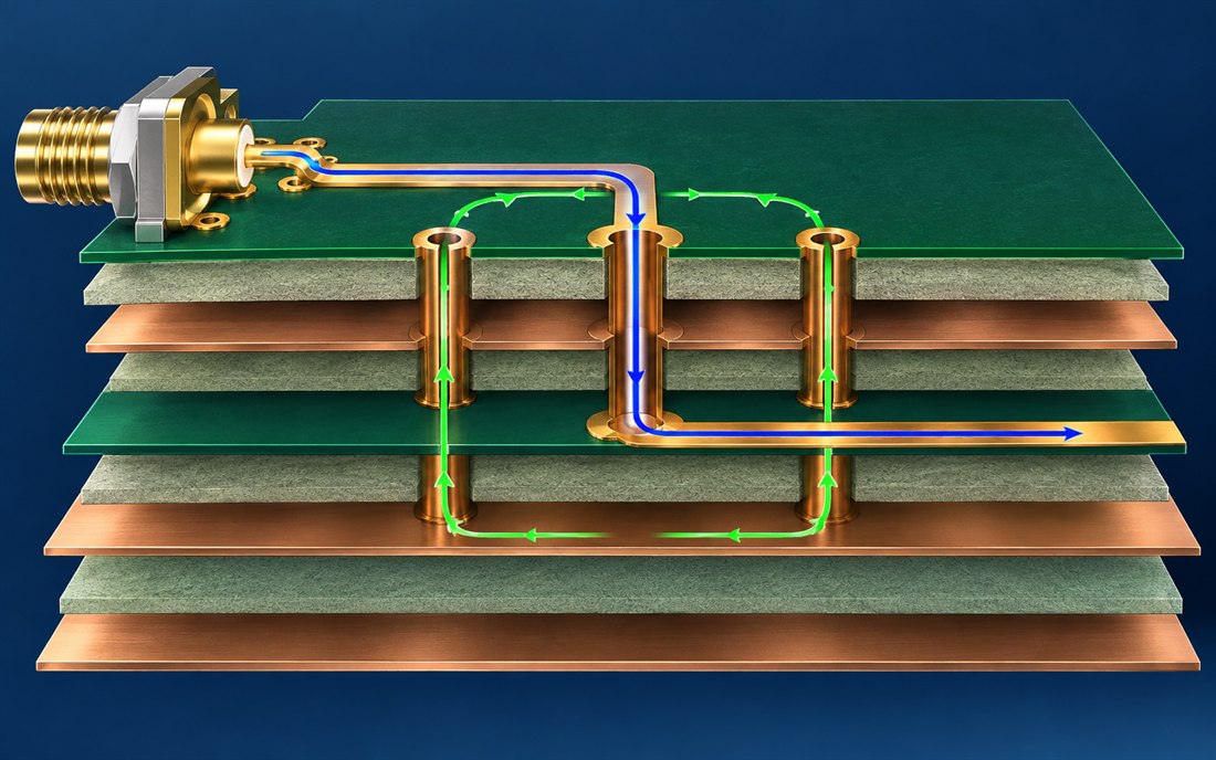
Satellite PCB Launch Design must identify which plane is the signal’s RF reference at the connector and where that reference changes through the channel. A solid plane directly beneath the launch is often more useful than adding vias mechanically around the connector without understanding their return-current role. Ground vias placed beside a signal transition can connect reference layers and reduce loop area, but the spacing and count are geometry-dependent. They are not a universal fence recipe. Analog Devices’ RF layout guidance emphasizes continuous reference planes and local ground connections; apply such guidance to the selected laminate, connector, frequency, and field solver model rather than treating it as a guaranteed result.
Use the same transition geometry across matched channels wherever the architecture allows it. Keep the signal pad, anti-pad, nearby ground vias, connector centerline, and launch-to-device routing consistent. The Satellite PCB layout should preserve the reference path across layer changes and avoid plane splits beneath the route. A ground-return structure can then be reviewed with the connector vendor’s land pattern and the stackup model, not in isolation.
Satellite PCB Launch Design: Manage layer transitions deliberately
When Satellite PCB Launch Design requires the RF path to move to another layer, treat the via-transition geometry, its antipad, return vias, unused via stubs, and reference-plane sequence as one transition. Prefer avoiding unnecessary RF layer changes; when a transition is needed, assess via barrel length and stub effects at the frequency of interest and use back-drilling or a different via structure only when the design and fabrication plan justify it. Do not copy a via diameter or spacing from an unrelated evaluation board: those values depend on dielectric thickness, copper geometry, stackup, and the adjoining launch.
For a multilayer Satellite PCB, the approved multilayer PCB stackup must name each signal and reference layer, dielectric construction, copper weight, and finished thickness. Manufacturing should receive the same layer map and via sequence used for the field-solver model. controlled impedance is not simply a nominal trace width: the design target must be tied to the actual construction, coupon method, and acceptance definition. The project team should resolve whether the requirement for a Satellite PCB applies to the line, the launch, or both.
Satellite PCB Launch Design: Release the design with measurable evidence
Satellite PCB Launch Design verification requires a useful coupon that represents the launch and transition being released, not merely a straight transmission line. A Satellite PCB design review should freeze the calibration reference planes and acceptance method before the coupon is ordered. Define the connector mounting datum, launch geometry, stackup, calibration reference plane, de-embedding approach if used, and the structures that the lab or customer will measure. TDR can reveal discontinuities, while a calibrated network-analyzer setup can characterize frequency-domain behavior. The measurement report should identify the fixture, calibration method, reference planes, sample configuration, and limits. Do not label an illustrative simulation or design target as a measured production result.
Prototype acceptance should compare matched channels under the same assembly condition. Record connector torque or fastening method where applicable, solder condition, board edge quality, and any rework. A prototype assembly that uses a different connector, stackup, or reflow sequence is not automatically a valid correlation sample for the production release. Coordinate the launch drawing with PCB assembly and SMT process controls so that the realized geometry is inspectable.
Satellite PCB Launch Design: A practical review sequence
- Freeze the connector part, board edge, mechanical datum, and enclosure contact.
- Document the complete stackup and RF reference plane at the launch and at every layer transition.
- Review signal pad, ground contacts, via/antipad geometry, stub strategy, and plane continuity in one model.
- Keep matched channels geometrically consistent and identify tuning or calibration allowances explicitly.
- Specify coupon geometry, calibration planes, TDR or VNA method, acceptance limits, and sample configuration.
- Release connector drawing, native layout, fabrication notes, and assembly requirements at one revision.
For a Satellite PCB Launch Design program manager, the key schedule risk is late discovery that the “connector issue” is actually a stackup, enclosure, or measurement-reference mismatch. A spacecraft interconnect release package should identify the design owner for each interface and distinguish model targets from measured acceptance. Where fabrication questions remain, a documented prototype build can close those questions before the channel geometry is frozen.
Sources: Analog Devices, “PCBs Layout Guidelines for RF & Mixed-Signal” and “High Fidelity PCB Design for Multichannel Beamformers—Part 1: Return Loss”; Qorvo, RF device thermal and evaluation-board application guidance. These references inform general design practice; no customer launch measurement or KKPCB test result is claimed here.





