
The probe cable is not an accessory that starts after the PCB is finished. In an ultrasound console, the cable shield, connector shell, strain-relief hardware, transmit return, and receive pair all meet at one mechanically active boundary. If that boundary is treated as a simple symbol in the schematic, cable movement can modulate shield current, the connector launch can convert common-mode energy, and a quiet receive channel can lose margin before the first patient-facing evaluation. This article treats the Ultrasound PCB probe interface as an electrical, mechanical, and manufacturing feature that must be released together. The Ultrasound PCB probe interface is the boundary where cable mechanics and receive-chain noise meet.
An Ultrasound PCB probe interface is most reliable when the team maps the cable current path before selecting the connector footprint. The examples below are design targets and engineering checks, not claims of a customer measurement. Confirm final pin pitch, current, flex life, cleaning chemistry, and impedance with the selected probe and connector data sheets.
- Treat the probe boundary as part of the circuit
- Build a connector launch that survives motion
- Make shield and return-current decisions explicit
- Release the mechanical and assembly details together
- Verify the interface before the first clinical build
Ultrasound PCB probe boundary as part of the circuit
The first design question is not “which connector fits the enclosure?” It is “where does the probe current return when the cable moves?” A probe assembly can carry high-voltage transmit pulses, low-level receive signals, identification lines, temperature sensing, and a shield braid in the same bundle. Those currents do not all want the same reference. A connector pinout that looks tidy in a schematic can place a fast transmit return beside a high-impedance receive pin, or force the shield through a long copper neck before it reaches the chassis datum.
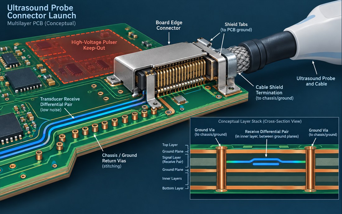
Start the Ultrasound PCB floorplan with three physical corridors: the transducer receive path, the pulser and T/R-switch path, and the connector-to-chassis transition. Mark the intended reference plane under each corridor and reserve the keep-outs before placing decoupling parts. The receive corridor should be short, symmetric, and protected from the connector’s mechanical mounting holes. The pulser corridor needs a defined return and clearance from sensitive inputs. The chassis transition needs a low-inductance shield path that does not borrow the analog reference through a narrow trace.
Separate signal ground from chassis intent
A shield termination is not automatically an analog-ground connection. In a medical instrument, the enclosure, cable braid, board ground, and protective-earth strategy can be related but are not interchangeable. Document the intended connection at the connector drawing, then repeat it in the PCB materials and stack-up notes so a copper pour revision does not silently change the return path.
For an early design review, ask each owner to answer four questions: Which current is expected on this shield? Which plane receives it first? What happens if the cable is touched or flexed? Where can a technician inspect the termination? This simple ownership table exposes boundary assumptions earlier than a late electromagnetic-compatibility review.
Build a connector launch that survives motion
A connector launch has two jobs. It must carry the intended signal with a controlled reference, and it must keep mechanical force away from fragile solder joints and plated features. The electrical launch should be reviewed in cross-section: connector pins, escape vias, reference plane, ground stitching, solder mask, and the enclosure datum. A top-view-only review can miss a return via that lands in a plane void or a mounting screw that overlaps a buried trace.
Use a Ultrasound PCB multilayer build when the interface needs a dedicated receive reference and a separate pulser or power layer. The exact dielectric thickness and copper weight should come from the fabricator’s controlled stack-up, not a generic library footprint. If the connector requires a broad ground pad, check whether the pad creates an unnecessary capacitive step for a fast receive transition. If the launch is single-ended, control its reference width; if it is differential, preserve pair symmetry through the connector escape.
Mechanical clearance is equally important. Keep the first bend of the cable outside the board edge datum and support the braid or shield with a bracket that transfers force to the enclosure or a rigid board area. Do not let a flexing cable pull directly on a row of fine-pitch solder joints. A practical PCB manufacturing release identifies an Ultrasound PCB probe interface datum before it identifies a cosmetic board feature. It identifies the bracket holes, board-edge keep-out, copper pullback, and acceptable fillet shape on the same drawing.
Design the cable bend envelope before routing
The cable bend envelope should be a real mechanical layer in the CAD release. Draw the minimum bend radius supplied by the cable vendor, then add the motion envelope expected during probe positioning, service access, and sterilization handling. Traces, test pads, and exposed copper must stay outside that envelope. If the cable can rotate around the connector, model the torsion direction as well as the simple left-to-right bend.
A rigid connector region can coexist with a flex tail or a small rigid-flex transition, but the transition needs its own strain-relief and copper-balancing rules. A PCB prototype that uses a temporary cable clamp is not enough evidence for a production release; the prototype should reproduce the intended datum and bracket load path.
Make shield and return-current decisions explicit
Shield continuity problems often appear as “random” receive noise because the electrical symptom changes with cable position. Replace that ambiguity with a current map. Show where the braid bonds to the connector shell, where the shell bonds to chassis, where chassis bonds to the enclosure, and where the board reference is allowed to meet that path. Use multiple short stitching connections when the connector geometry supports them, but avoid a long loop that forces shield current through the quiet receive plane.
The return path also includes mounting hardware. A metal bracket, spring finger, or mounting screw can become part of the RF path. Add those parts to the high-frequency PCB review and specify the surface finish, contact pressure, and plating compatibility. If a bracket is painted, a nominally grounded screw may not provide a repeatable connection. If a spring finger is used, define its compression window and inspection access.
Keep the pulser return and the receiver return distinct until the intended reference point. In an Ultrasound PCB probe interface, that separation is easier to inspect when the connector and shield datums are on the same drawing. The high-voltage path should have a compact loop, a clear creepage strategy, and a controlled transition into the connector. The receive input should not cross that loop’s return via field. When a layer transition is unavoidable, use a matched via arrangement and place nearby ground stitching so the reference does not detour.
Use manufacturable geometry, not idealized copper
Connector launch rules must survive etch, plating, solder mask, and assembly tolerance. Ask the fabricator for finished hole size, annular-ring capability, copper pullback, and the actual board-edge tolerance. For a dense controlled-impedance PCB interface, include the finished dielectric and solder-mask assumptions in the impedance table. If the supplier proposes a different stack-up, re-check the launch geometry rather than accepting a verbal equivalence.
Surface finish is also part of the interface. Choose a finish that supports the connector contact system, repeated mating, and the required cleaning process. Document whether exposed edge contacts are beveled, plated, masked, or protected by a mechanical guide. A PCB fabrication note that omits this detail can leave purchasing with a material substitution that changes contact wear and insertion force.
Release the mechanical and assembly details together
The connector footprint, bracket, cable jacket, and board assembly process should be released as one package. The Ultrasound PCB probe interface should carry those assembly assumptions into the inspection plan. During PCB assembly, a large connector can shadow nearby components, trap flux, or prevent optical inspection of a row of contacts. Define stencil apertures, paste reduction, reflow orientation, hand-solder operations, and the order in which the bracket is installed. If a bracket is fastened after reflow, verify that its torque cannot bow the board or crack a nearby ceramic capacitor.
Cleaning and coating deserve a project-level decision. Some probe assemblies require a wipe-down or low-residue process rather than immersion. State which surfaces must remain free of coating, which connector cavities need masking, and how the inspection team confirms that no residue remains under the bracket. The second illustration below is a conceptual inspection workflow, not a claim of a measured cleanliness result.
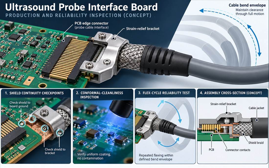
A serviceable PCBA should expose a safe probe and shield inspection point without requiring technicians to pry against the cable. Add a connector datum to the assembly drawing, identify the acceptable contact wipe, and show where a probe fixture can rest without loading the solder joints. These details reduce field-rework variation and keep the electrical launch consistent from prototype to production.
Plan for change control at the probe boundary
Connector substitutions are not drop-in changes when pin pitch, shell height, shield contact, or cable exit direction changes. A revision request should trigger an impact check for pinout, return current, bend envelope, mounting torque, creepage, stencil access, and test-fixture compatibility. Record the decision in the PCB design release package, not only in a supplier email.
If the probe vendor changes the cable construction, repeat the mechanical clearance and shield-bond review. If firmware adds a probe-ID bus, review its pull-up return and switching edges near the receive corridor. The project manager should treat these as interface dependencies with owners and due dates, not as late documentation tasks.
Verify the interface before the first clinical build
Use a five-pass verification plan. Pass one checks the connector pinout and probe polarity against the approved cable drawing. Pass two follows shield and return current through the shell, bracket, board, and enclosure datum. Pass three checks every receive and pulser transition against the stack-up and keep-out map. Pass four reviews assembly access, cleaning masks, stencil constraints, and torque notes. Pass five confirms that a test fixture can measure shield continuity, contact resistance, and the intended receive reference without disturbing the cable.
For the first board, separate targets from evidence. “Maintain the specified contact geometry through the connector launch” is a design requirement. A claim about noise, insertion loss, or flex life requires a defined fixture, method, and recorded result. The PCB testing plan should identify which measurements are coupon-based, which are board-level, and which are mechanical checks. That distinction keeps the release credible and makes an out-of-range result actionable.
The Ultrasound PCB interface package should be reviewed with the RF return map before the final handoff. The final handoff should include the approved stack-up. An Ultrasound PCB probe interface release is complete only when the cable, connector, and board owners can trace the same return path. The final handoff should include the approved stack-up, connector and cable drawings, shield-bond diagram, bend envelope, mounting torque, surface-finish callout, cleaning instructions, inspection images, and change-control owner. When those files travel together, an Ultrasound PCB probe interface can move from engineering prototype to repeatable assembly without relying on an undocumented “good enough” connector launch.
A reliable probe boundary is not created by adding more copper after a noise complaint. It comes from assigning the return path, mechanical load path, cleaning method, and inspection method before the first panel is released. For engineers, that means routing the connector and shield as part of the receive system. For project managers, it means closing the cable, enclosure, fixture, and assembly dependencies before committing to a clinical build.
Sources: selected probe, cable, connector, ADC, and pulser data sheets; approved PCB material and fabrication data; assembly and cleaning process instructions; and engineering guidance from Analog Devices, Qorvo, Würth Elektronik, and relevant RF/medical PCB references. Values and checks in this article are design targets or engineering methods, not customer measurement claims.
